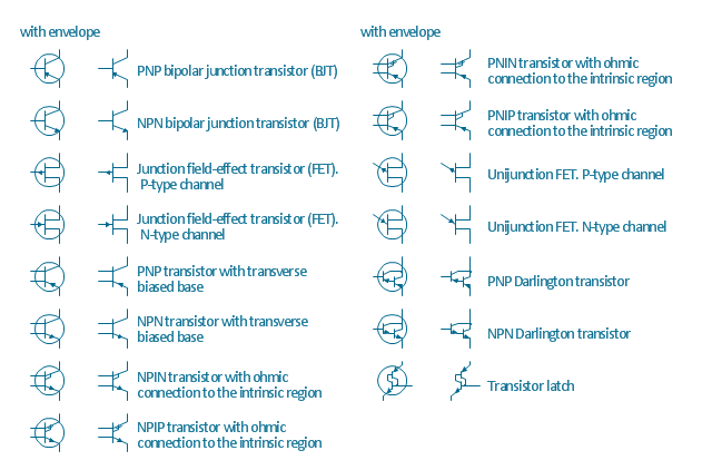
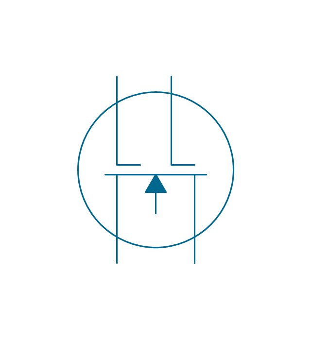
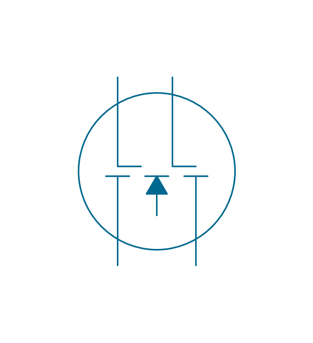
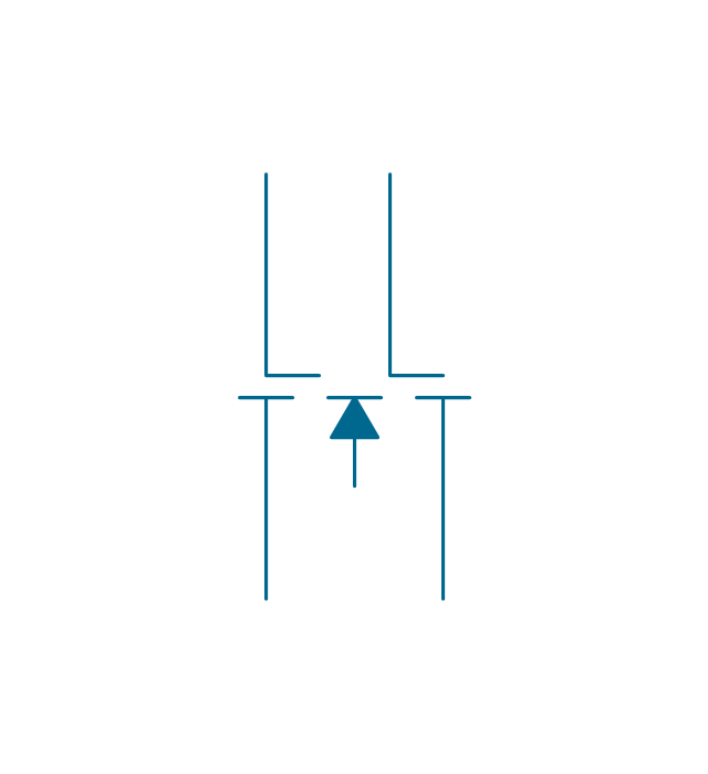
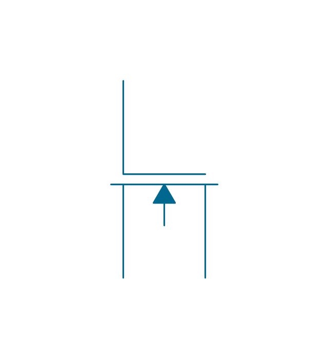
Electrical Symbols — Transistors

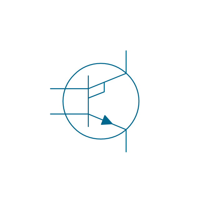
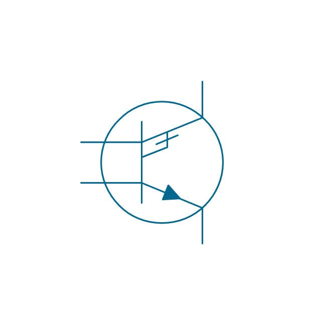
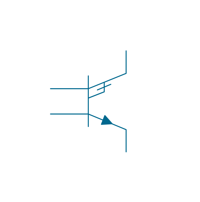
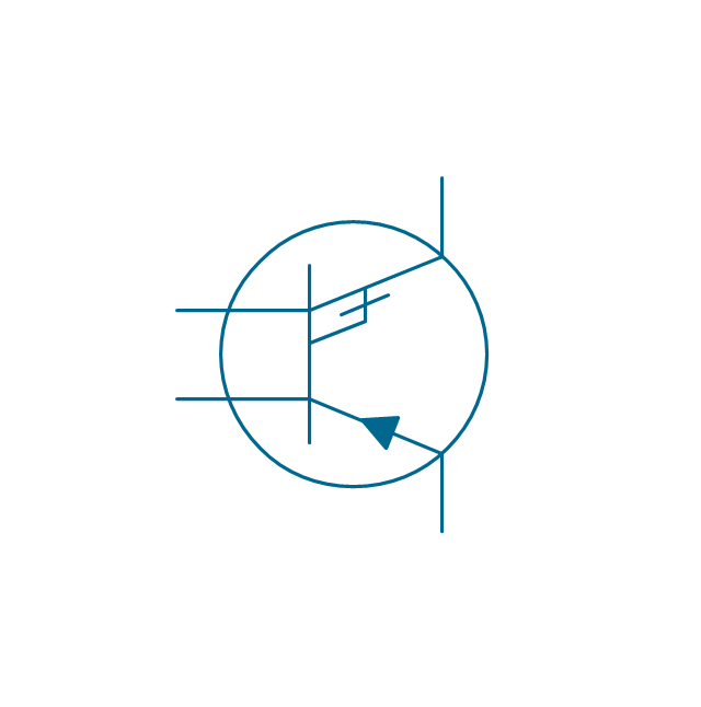
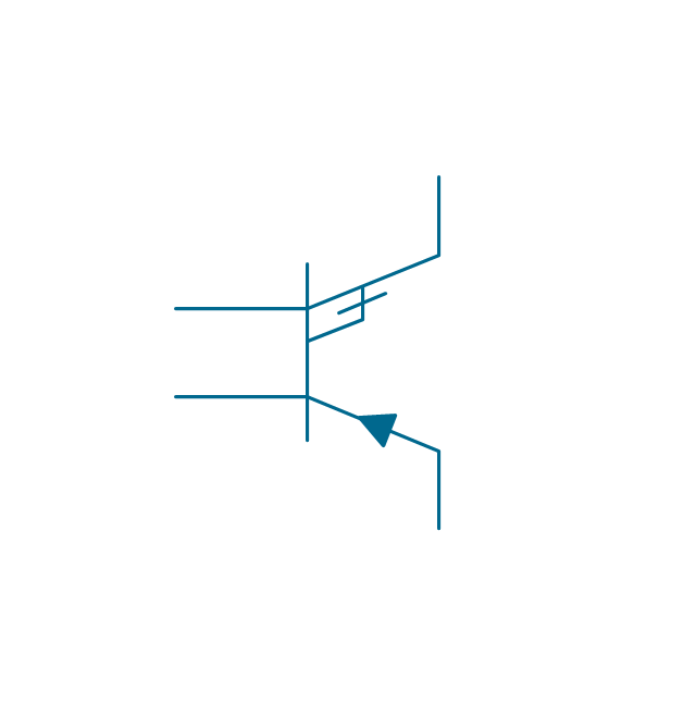
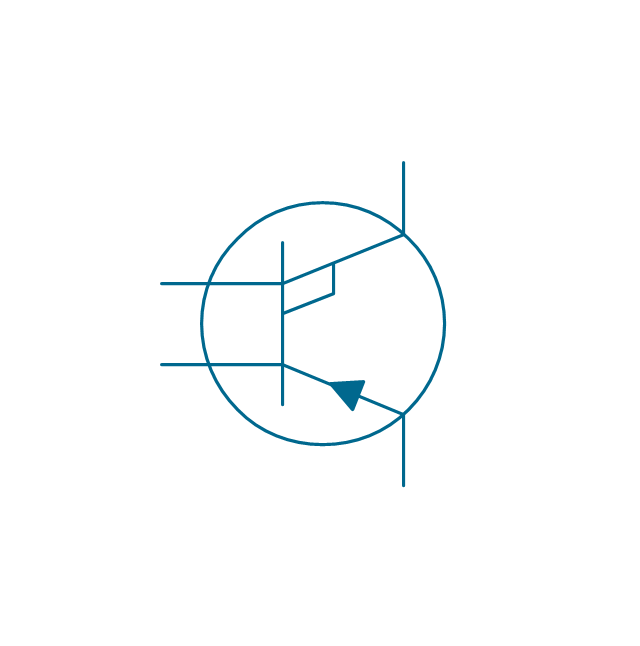
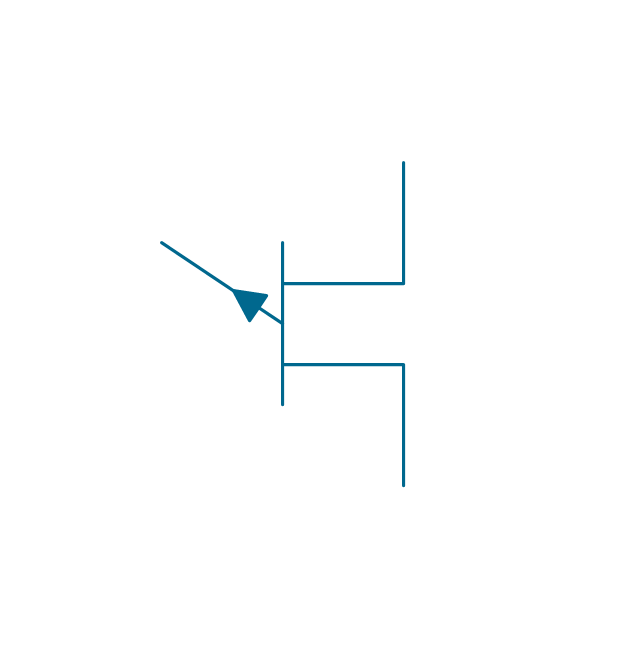
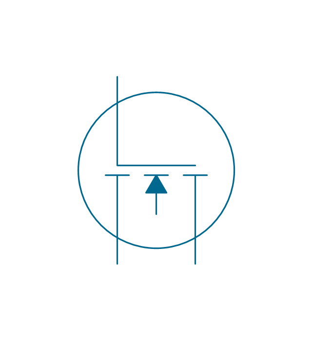
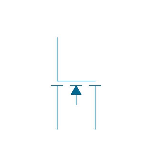
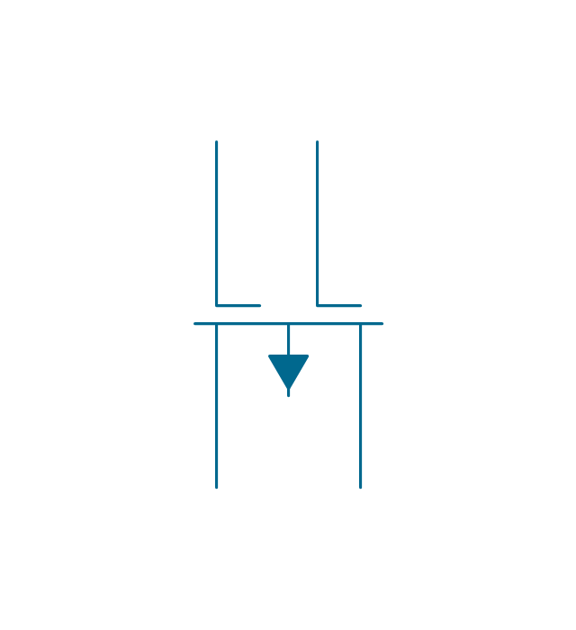
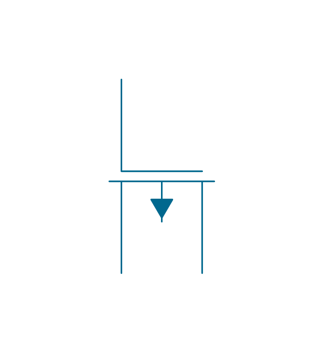
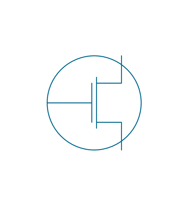
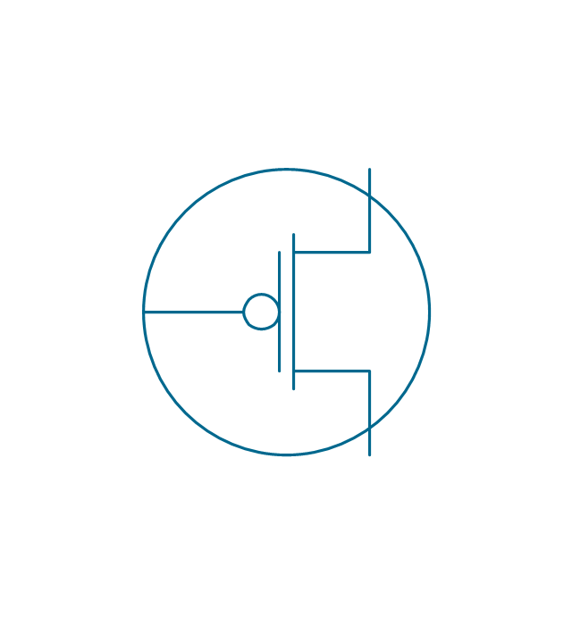
The vector stencils library "Transistors" contains 30 symbols of transistors.
Use these shapes for drawing electronic schematics and circuit diagrams in the ConceptDraw PRO diagramming and vector drawing software extended with the Electrical Engineering solution from the Engineering area of ConceptDraw Solution Park.
www.conceptdraw.com/ solution-park/ engineering-electrical
Use these shapes for drawing electronic schematics and circuit diagrams in the ConceptDraw PRO diagramming and vector drawing software extended with the Electrical Engineering solution from the Engineering area of ConceptDraw Solution Park.
www.conceptdraw.com/ solution-park/ engineering-electrical
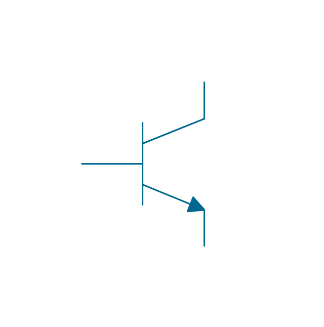
BJT, PNP, env
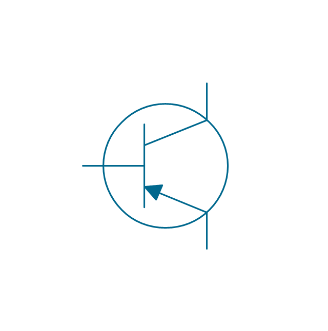
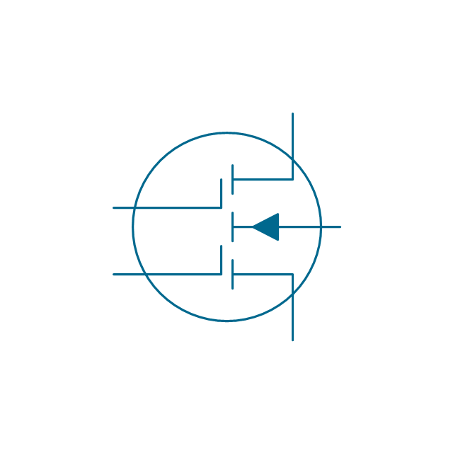
BJT, PNP
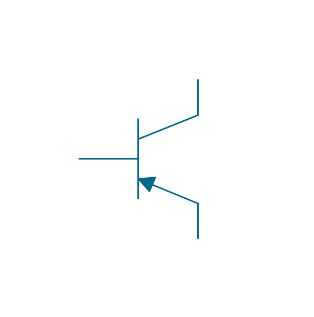
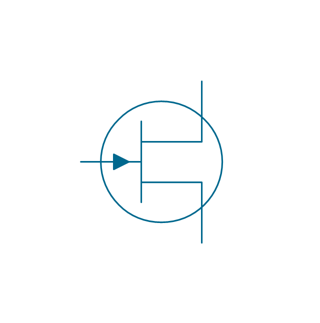
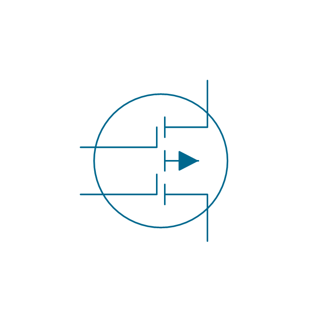
BJT, NPN, env
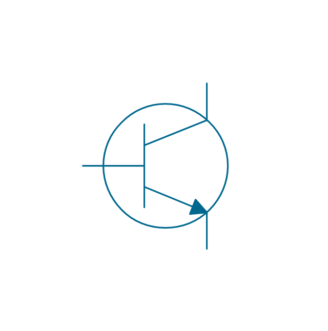
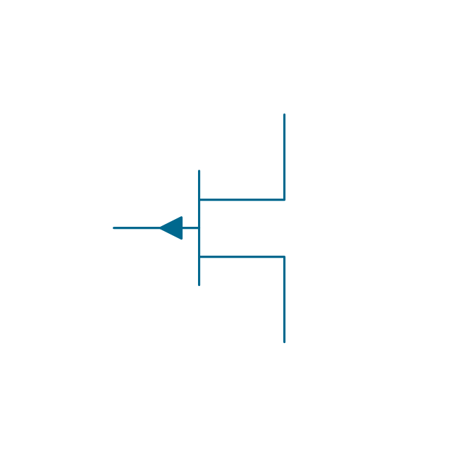
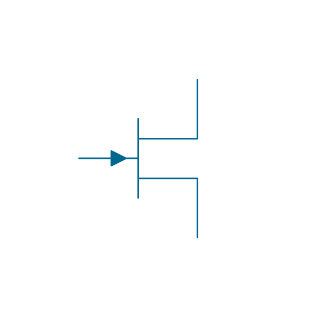
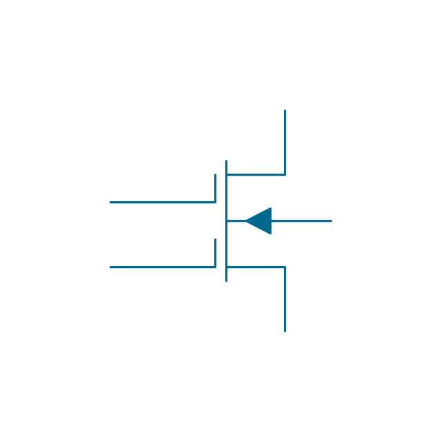
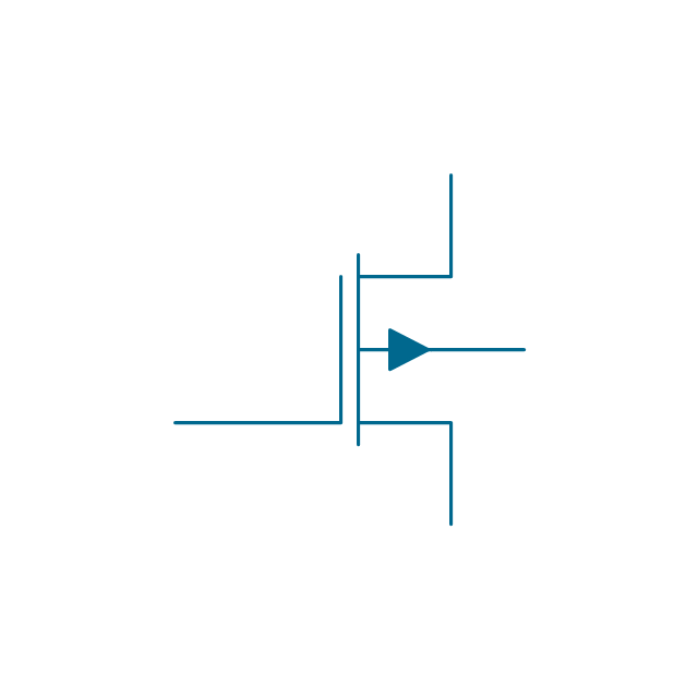
BJT, NPN
JFET, P, env

JFET, P
JFET, N, env
JFET, N
Transverse biased base, PNP, env

Transverse biased base, PNP
Transverse biased base, NPN, env

Transverse biased base, NPN

Ohmic, NPIN, env
Ohmic, NPIN

Ohmic, NPIP, env
Ohmic, NPIP
Ohmic, PNIN, env
Ohmic, PNIN
Ohmic, PNIP, env
Ohmic, PNIP

Unijunction FET, P, env

Unijunction FET, P
Unijunction FET, N, env

Unijunction FET, N

Darlington transistor, PNP, env
Darlington transistor, PNP
Darlington transistor, NPN, env
Darlington transistor, NPN

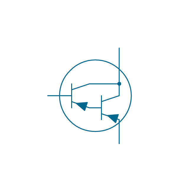
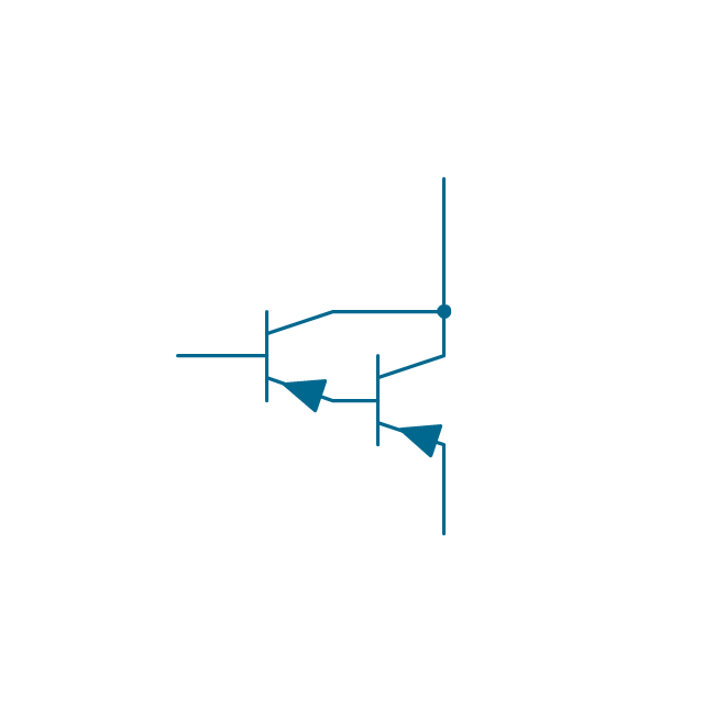
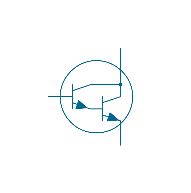
Transistor latch, env
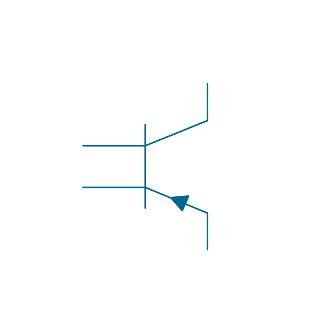
Transistor latch
The vector stencils library "Transistors" contains 30 symbols of transistors drawing electronic schematics and circuit diagrams.
"A transistor is a semiconductor device used to amplify and switch electronic signals and electrical power. It is composed of semiconductor material with at least three terminals for connection to an external circuit. A voltage or current applied to one pair of the transistor's terminals changes the current through another pair of terminals. Because the controlled (output) power can be higher than the controlling (input) power, a transistor can amplify a signal. Today, some transistors are packaged individually, but many more are found embedded in integrated circuits.
The transistor is the fundamental building block of modern electronic devices, and is ubiquitous in modern electronic systems. ...
Transistors are categorized by:
(1) Semiconductor material...: the metalloids germanium ... and silicon ... in amorphous, polycrystalline and monocrystalline form; the compounds gallium arsenide ... and silicon carbide ..., the alloy silicon-germanium ..., the allotrope of carbon graphene ...
(2) Structure: BJT, JFET, IGFET (MOSFET), insulated-gate bipolar transistor, "other types"
(3) Electrical polarity (positive and negative): n–p–n, p–n–p (BJTs); n-channel, p-channel (FETs)
(4) Maximum power rating: low, medium, high
(5) Maximum operating frequency: low, medium, high, radio (RF), microwave frequency...
(6) Application: switch, general purpose, audio, high voltage, super-beta, matched pair
(7) Physical packaging: through-hole metal, through-hole plastic, surface mount, ball grid array, power modules...
(8) Amplification factor..." [Transistor. Wikipedia]
The shapes example "Design elements - Transistors" was drawn using the ConceptDraw PRO diagramming and vector drawing software extended with the Electrical Engineering solution from the Engineering area of ConceptDraw Solution Park.
Transistor symbols
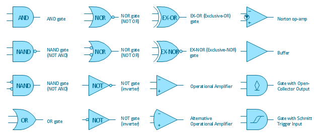
The vector stencils library "Logic gate diagram" contains 17 element symbols for drawing the logic gate diagrams.
"To build a functionally complete logic system, relays, valves (vacuum tubes), or transistors can be used. The simplest family of logic gates using bipolar transistors is called resistor-transistor logic (RTL). Unlike simple diode logic gates (which do not have a gain element), RTL gates can be cascaded indefinitely to produce more complex logic functions. RTL gates were used in early integrated circuits. For higher speed and better density, the resistors used in RTL were replaced by diodes resulting in diode-transistor logic (DTL). Transistor-transistor logic (TTL) then supplanted DTL. As integrated circuits became more complex, bipolar transistors were replaced with smaller field-effect transistors (MOSFETs); see PMOS and NMOS. To reduce power consumption still further, most contemporary chip implementations of digital systems now use CMOS logic. CMOS uses complementary (both n-channel and p-channel) MOSFET devices to achieve a high speed with low power dissipation." [Logic gate. Wikipedia]
The symbols example "Design elements - Logic gate diagram" was drawn using the ConceptDraw PRO diagramming and vector drawing software extended with the Electrical Engineering solution from the Engineering area of ConceptDraw Solution Park.
Logic gate symbols
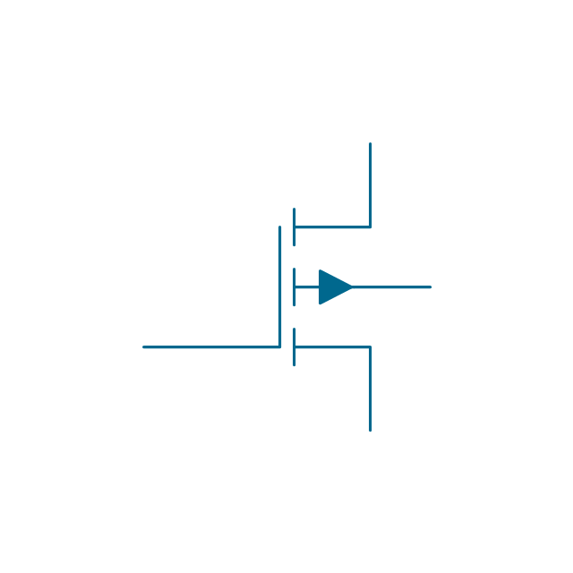
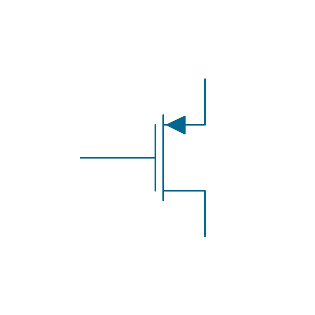
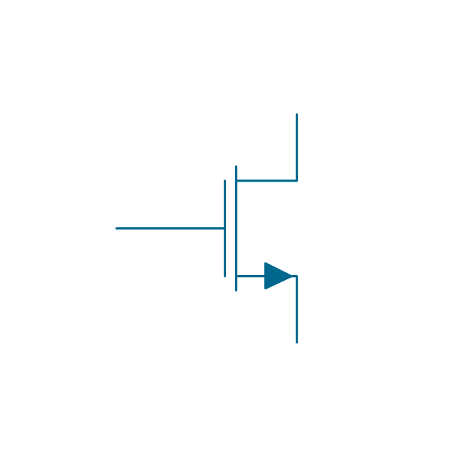
The vector stencils library "IGFET" contains 18 symbols of IGFET (insulated-gate field-effect transistor) elements for drawing electronic circuit diagrams.
"The metal–oxide–semiconductor field-effect transistor (MOSFET, MOS-FET, or MOS FET) is a transistor used for amplifying or switching electronic signals. Although the MOSFET is a four-terminal device with source (S), gate (G), drain (D), and body (B) terminals, the body (or substrate) of the MOSFET often is connected to the source terminal, making it a three-terminal device like other field-effect transistors. Because these two terminals are normally connected to each other (short-circuited) internally, only three terminals appear in electrical diagrams. The MOSFET is by far the most common transistor in both digital and analog circuits, though the bipolar junction transistor was at one time much more common. ...
An insulated-gate field-effect transistor or IGFET is a related term almost synonymous with MOSFET. The term may be more inclusive, since many "MOSFETs" use a gate that is not metal, and a gate insulator that is not oxide. Another synonym is MISFET for metal–insulator–semiconductor FET." [MOSFET
From Wikipedia]
The symbols example "Design elements - IGFET" was drawn using the ConceptDraw PRO diagramming and vector drawing software extended with the Electrical Engineering solution from the Engineering area of ConceptDraw Solution Park.
IGFET elements

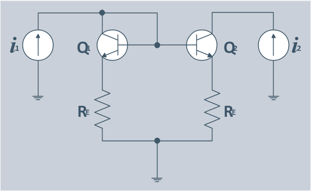
The circuit diagram example "Bipolar current mirror" was redesigned from the Wikipedia file: Current mirror.png.
[en.wikipedia.org/ wiki/ File:Current_ mirror.png]
This file is licensed under the Creative Commons Attribution-Share Alike 3.0 Unported license. [creativecommons.org/ licenses/ by-sa/ 3.0/ deed.en]
"A current mirror is a circuit designed to copy a current through one active device by controlling the current in another active device of a circuit, keeping the output current constant regardless of loading. The current being 'copied' can be, and sometimes is, a varying signal current. Conceptually, an ideal current mirror is simply an ideal inverting current amplifier that reverses the current direction as well or it is a current-controlled current source (CCCS). The current mirror is used to provide bias currents and active loads to circuits. ...
Basic BJT current mirror.
If a voltage is applied to the BJT base-emitter junction as an input quantity and the collector current is taken as an output quantity, the transistor will act as an exponential voltage-to-current converter. By applying a negative feedback (simply joining the base and collector) the transistor can be "reversed" and it will begin acting as the opposite logarithmic current-to-voltage converter; now it will adjust the "output" base-emitter voltage so as to pass the applied "input" collector current.
The simplest bipolar current mirror ... implements this idea. It consists of two cascaded transistor stages acting accordingly as a reversed and direct voltage-to-current converters." [Current mirror. Wikipedia]
The circuit diagram example "Bipolar current mirror" was created using the ConceptDraw PRO diagramming and vector drawing software extended with the Electrical Engineering solution from the Engineering area of ConceptDraw Solution Park.
Circuit diagram
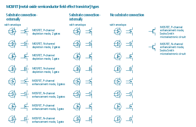
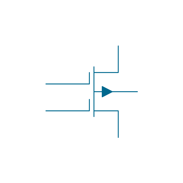
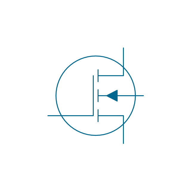
The vector stencils library "MOSFET" contains 18 symbols of MOSFET (metal–oxide–semiconductor field-effect transistor) elements for drawing electronic circuits diagrams.
"A variety of symbols are used for the MOSFET. The basic design is generally a line for the channel with the source and drain leaving it at right angles and then bending back at right angles into the same direction as the channel. Sometimes three line segments are used for enhancement mode and a solid line for depletion mode. ... Another line is drawn parallel to the channel for the gate.
The "bulk" or "body" connection, if shown, is shown connected to the back of the channel with an arrow indicating PMOS or NMOS. Arrows always point from P to N, so an NMOS (N-channel in P-well or P-substrate) has the arrow pointing in (from the bulk to the channel). If the bulk is connected to the source (as is generally the case with discrete devices) it is sometimes angled to meet up with the source leaving the transistor. If the bulk is not shown (as is often the case in IC design as they are generally common bulk) an inversion symbol is sometimes used to indicate PMOS, alternatively an arrow on the source may be used in the same way as for bipolar transistors (out for nMOS, in for pMOS). ...
For the symbols in which the bulk, or body, terminal is shown, it is here shown internally connected to the source... This is a typical configuration, but by no means the only important configuration. In general, the MOSFET is a four-terminal device, and in integrated circuits many of the MOSFETs share a body connection, not necessarily connected to the source terminals of all the transistors." [MOSFET. Wikipedia]
The symbols example "Design elements - MOSFET" was drawn using the ConceptDraw PRO diagramming and vector drawing software extended with the Electrical Engineering solution from the Engineering area of ConceptDraw Solution Park.
MOSFET symbols
Electrical Symbols — MOSFET

The vector stencils library "IGFET" contains 18 symbols of IGFET (insulated-gate field-effect transistor) elements.
Use these shapes for drawing electronic circuit diagrams in the ConceptDraw PRO diagramming and vector drawing software extended with the Electrical Engineering solution from the Engineering area of ConceptDraw Solution Park.
www.conceptdraw.com/ solution-park/ engineering-electrical
Use these shapes for drawing electronic circuit diagrams in the ConceptDraw PRO diagramming and vector drawing software extended with the Electrical Engineering solution from the Engineering area of ConceptDraw Solution Park.
www.conceptdraw.com/ solution-park/ engineering-electrical
IGFET, N, dep, 2 gates, env
IGFET, N, dep, 2 gates

IGFET, N, enh, 2 gates, env
IGFET, N, enh, 2 gates
IGFET, N, dep, 1 gate, env

IGFET, N, dep, 1 gate
IGFET, N, enh, 1 gate, env
IGFET, N, enh, 1 gate, env
IGFET, P, dep, 2 gates, env

IGFET, P, dep, 2 gates
IGFET, P, enh, 2 gates, env

IGFET, P, enh, 2 gates

IGFET, P, dep, 1 gate, env

IGFET, P, dep, 1 gate
IGFET, P, enh, 1 gate, env

IGFET, P, enh, 1 gate

IGFET, N, enh
IGFET, P, enh
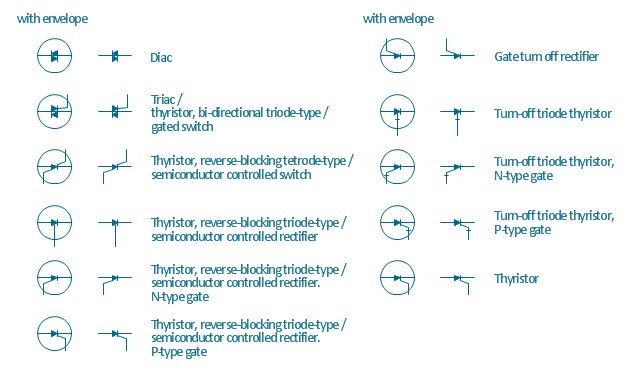
The vector stencils library "Semiconductors" contains 22 symbols of rectifiers, diodes, charge transfer and electronic conduction devices, switches, cathodes, transistors, thyristors, and transceivers for semiconductor (SIS) design.
"Semiconductor devices are electronic components that exploit the electronic properties of semiconductor materials, principally silicon, germanium, and gallium arsenide, as well as organic semiconductors. Semiconductor devices have replaced thermionic devices (vacuum tubes) in most applications. They use electronic conduction in the solid state as opposed to the gaseous state or thermionic emission in a high vacuum.
Semiconductor devices are manufactured both as single discrete devices and as integrated circuits (ICs), which consist of a number - from a few (as low as two) to billions - of devices manufactured and interconnected on a single semiconductor substrate, or wafer. ...
All transistor types can be used as the building blocks of logic gates, which are fundamental in the design of digital circuits. In digital circuits like microprocessors, transistors act as on-off switches; in the MOSFET, for instance, the voltage applied to the gate determines whether the switch is on or off.
Transistors used for analog circuits do not act as on-off switches; rather, they respond to a continuous range of inputs with a continuous range of outputs. Common analog circuits include amplifiers and oscillators.
Circuits that interface or translate between digital circuits and analog circuits are known as mixed-signal circuits.
Power semiconductor devices are discrete devices or integrated circuits intended for high current or high voltage applications. Power integrated circuits combine IC technology with power semiconductor technology, these are sometimes referred to as "smart" power devices. Several companies specialize in manufacturing power semiconductors." [Semiconductor device. Wikipedia]
The shapes example "Design elements - Semiconductors" was drawn using the ConceptDraw PRO diagramming and vector drawing software extended with the Electrical Engineering solution from the Engineering area of ConceptDraw Solution Park.
Semiconductor elements
Electrical Symbols — IGFET

EPC Engineering

The vector stencils library "MOSFET" contains 18 symbols of MOSFET (metal–oxide–semiconductor field-effect transistor) elements.
Use these shapes for drawing electronic circuits diagrams in the ConceptDraw PRO diagramming and vector drawing software extended with the Electrical Engineering solution from the Engineering area of ConceptDraw Solution Park.
www.conceptdraw.com/ solution-park/ engineering-electrical
Use these shapes for drawing electronic circuits diagrams in the ConceptDraw PRO diagramming and vector drawing software extended with the Electrical Engineering solution from the Engineering area of ConceptDraw Solution Park.
www.conceptdraw.com/ solution-park/ engineering-electrical
MOSFET, P, dep, 2 gates, env

MOSFET, P, dep, 2 gates
MOSFET, N, dep, 2 gates, env

MOSFET, N, dep, 2 gates
MOSFET, P, dep, 1 gate, env

MOSFET, P, dep, 1 gate
MOSFET, N, dep, 1 gate, env

MOSFET, N, dep, 1 gate

MOSFET, P, enh, 2 gates, env
MOSFET, P, enh, 2 gates

MOSFET, N, enh, 2 gates, env
MOSFET, N, enh, 2 gates

MOSFET, P, enh, 1 gate, env

MOSFET, P, enh, 1 gate
MOSFET, N, enh, 1 gate, env
MOSFET, N, enh, 1 gate

MOSFET, P, enh, Sedra
MOSFET, N, enh, Sedra
Electrical Drawing Software and Electrical Symbols

Electrical Engineering

Electrical Symbols, Electrical Diagram Symbols

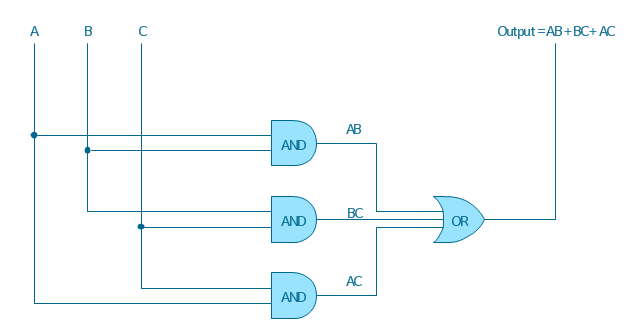
"A logic gate is an idealized or physical device implementing a Boolean function, that is, it performs a logical operation on one or more logical inputs, and produces a single logical output. Depending on the context, the term may refer to an ideal logic gate, one that has for instance zero rise time and unlimited fan-out, or it may refer to a non-ideal physical device...
Logic gates are primarily implemented using diodes or transistors acting as electronic switches, but can also be constructed using electromagnetic relays (relay logic), fluidic logic, pneumatic logic, optics, molecules, or even mechanical elements. With amplification, logic gates can be cascaded in the same way that Boolean functions can be composed, allowing the construction of a physical model of all of Boolean logic, and therefore, all of the algorithms and mathematics that can be described with Boolean logic.
Logic circuits include such devices as multiplexers, registers, arithmetic logic units (ALUs), and computer memory, all the way up through complete microprocessors, which may contain more than 100 million gates. In practice, the gates are made from field-effect transistors (FETs), particularly MOSFETs (metal–oxide–semiconductor field-effect transistors).
Compound logic gates AND-OR-Invert (AOI) and OR-AND-Invert (OAI) are often employed in circuit design because their construction using MOSFETs is simpler and more efficient than the sum of the individual gates.
In reversible logic, Toffoli gates are used." [Logic gate. Wikipedia]
The logic gate diagram template for the ConceptDraw PRO diagramming and vector drawing software is included in the Electrical Engineering solution from the Engineering area of ConceptDraw Solution Park.
Logic gate diagram
Electrical Diagram

Electrical Symbols — Thermo

Electrical Design Software

- Drawing Transistors With Visio
- Electrical Symbols — Transistors | Design elements - Transistors ...
- Transistors - Vector stencils library
- Electrical Symbols — Transistors | Electrical Symbols — MOSFET ...
- Design elements - Transistors | Transistors - Vector stencils library ...
- Design elements - Transistors
- Bipolar current mirror - Circuit diagram | Transistors - Vector stencils ...
- Design elements - Transistors | Design elements - Electron tubes ...
- Design elements - Transistors | ConceptDraw Arrows10 Technology ...
- Design elements - Transistors | Design elements - Semiconductor ...
- Electrical Symbols — Transistors | Electrical Symbols ...
- Design elements - Resistors | Design elements - Transistors ...
- Electrical Symbols — VHF UHF SHF | Design elements - Transistors ...
- Electrical Symbols, Electrical Diagram Symbols | Electrical Symbols ...
- Metal Oxide Semiconductor Field Effect Transistor
- Electrical Symbols — Semiconductor | Electrical Symbols, Electrical ...
- Design elements - Semiconductor diodes | Design elements ...
- Design elements - Logic gate diagram | Symbol Amplifier Diagram
- Design elements - Logic gate diagram | Design elements - Analog ...
- Design elements - Logic gate diagram | Engineering | 2-bit ALU ...