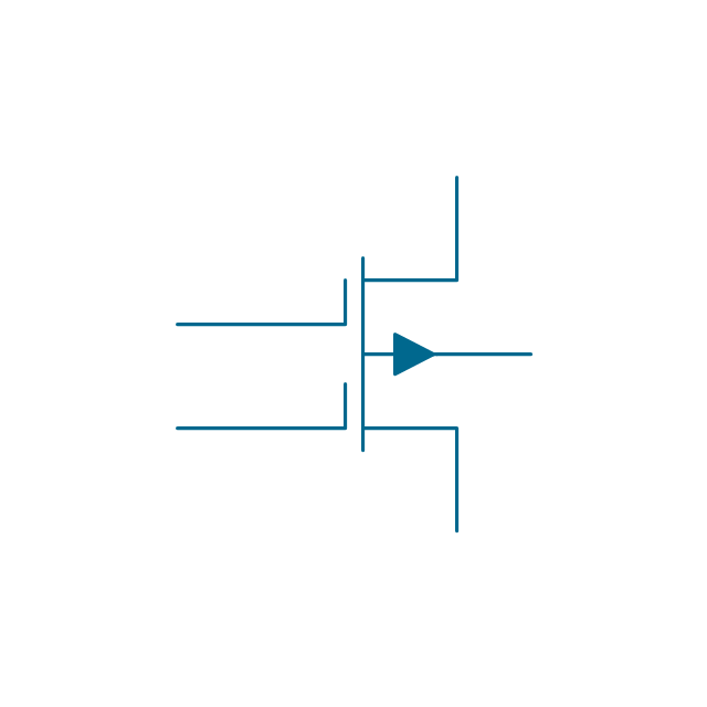
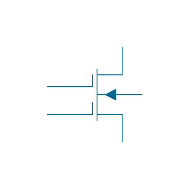
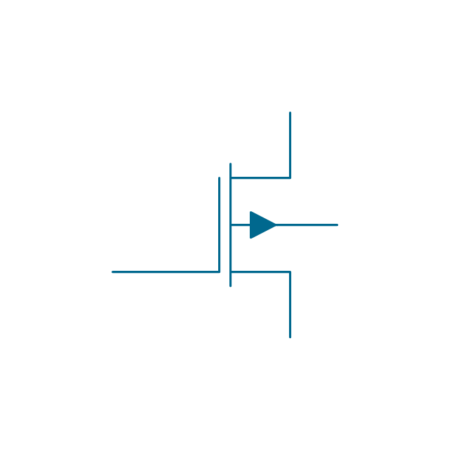
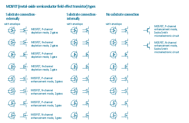
The vector stencils library "MOSFET" contains 18 symbols of MOSFET (metal–oxide–semiconductor field-effect transistor) elements.
Use these shapes for drawing electronic circuits diagrams in the ConceptDraw PRO diagramming and vector drawing software extended with the Electrical Engineering solution from the Engineering area of ConceptDraw Solution Park.
www.conceptdraw.com/ solution-park/ engineering-electrical
Use these shapes for drawing electronic circuits diagrams in the ConceptDraw PRO diagramming and vector drawing software extended with the Electrical Engineering solution from the Engineering area of ConceptDraw Solution Park.
www.conceptdraw.com/ solution-park/ engineering-electrical
MOSFET, P, dep, 2 gates, env

MOSFET, P, dep, 2 gates
MOSFET, N, dep, 2 gates, env

MOSFET, N, dep, 2 gates
MOSFET, P, dep, 1 gate, env
MOSFET, P, dep, 1 gate
MOSFET, N, dep, 1 gate, env

MOSFET, N, dep, 1 gate

MOSFET, P, enh, 2 gates, env
MOSFET, P, enh, 2 gates

MOSFET, N, enh, 2 gates, env
MOSFET, N, enh, 2 gates

MOSFET, P, enh, 1 gate, env

MOSFET, P, enh, 1 gate
MOSFET, N, enh, 1 gate, env
MOSFET, N, enh, 1 gate

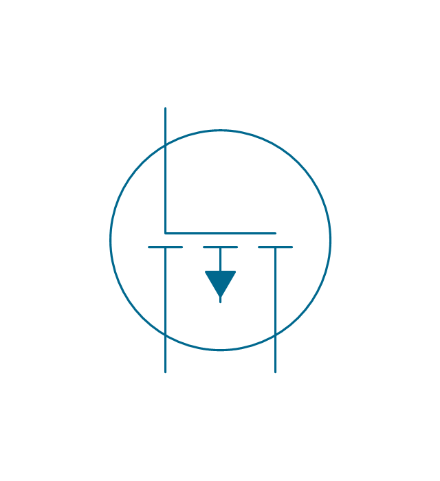
MOSFET, P, enh, Sedra
MOSFET, N, enh, Sedra
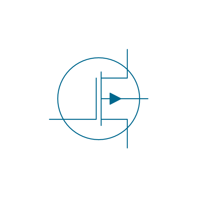
The vector stencils library "IGFET" contains 18 symbols of IGFET (insulated-gate field-effect transistor) elements.
Use these shapes for drawing electronic circuit diagrams in the ConceptDraw PRO diagramming and vector drawing software extended with the Electrical Engineering solution from the Engineering area of ConceptDraw Solution Park.
www.conceptdraw.com/ solution-park/ engineering-electrical
Use these shapes for drawing electronic circuit diagrams in the ConceptDraw PRO diagramming and vector drawing software extended with the Electrical Engineering solution from the Engineering area of ConceptDraw Solution Park.
www.conceptdraw.com/ solution-park/ engineering-electrical
IGFET, N, dep, 2 gates, env
IGFET, N, dep, 2 gates

IGFET, N, enh, 2 gates, env
IGFET, N, enh, 2 gates
IGFET, N, dep, 1 gate, env

IGFET, N, dep, 1 gate
IGFET, N, enh, 1 gate, env
IGFET, N, enh, 1 gate, env
IGFET, P, dep, 2 gates, env
IGFET, P, dep, 2 gates
IGFET, P, enh, 2 gates, env

IGFET, P, enh, 2 gates

IGFET, P, dep, 1 gate, env
IGFET, P, dep, 1 gate
IGFET, P, enh, 1 gate, env
IGFET, P, enh, 1 gate

IGFET, N, enh
IGFET, P, enh
The vector stencils library "MOSFET" contains 18 symbols of MOSFET (metal–oxide–semiconductor field-effect transistor) elements for drawing electronic circuits diagrams.
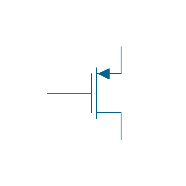
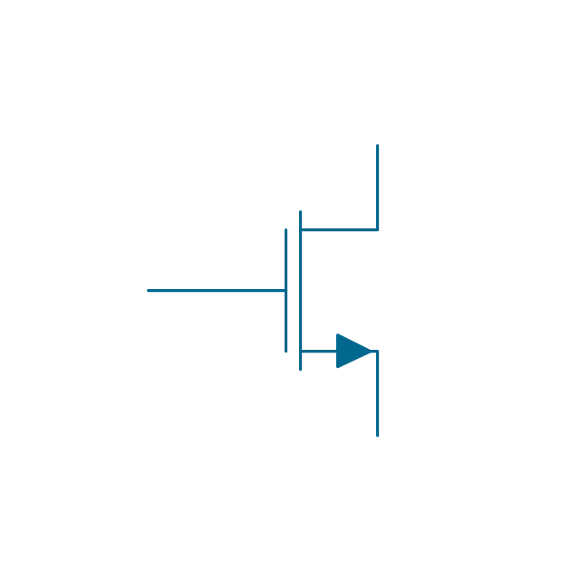
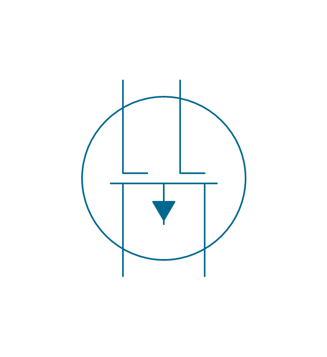
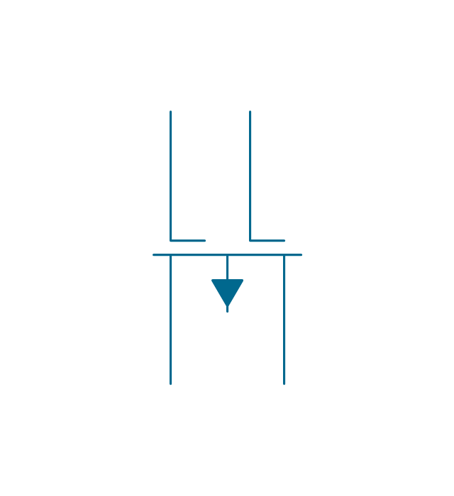
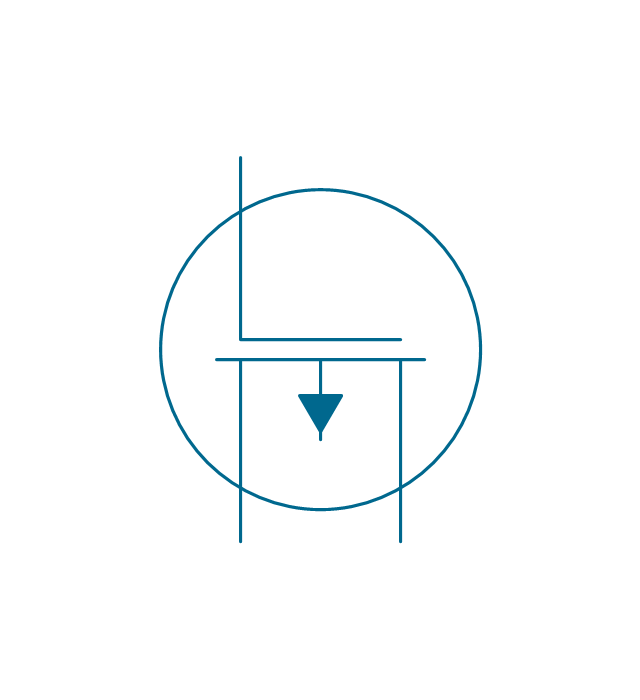
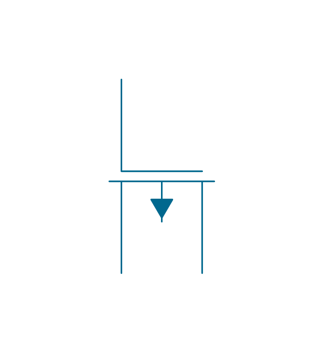
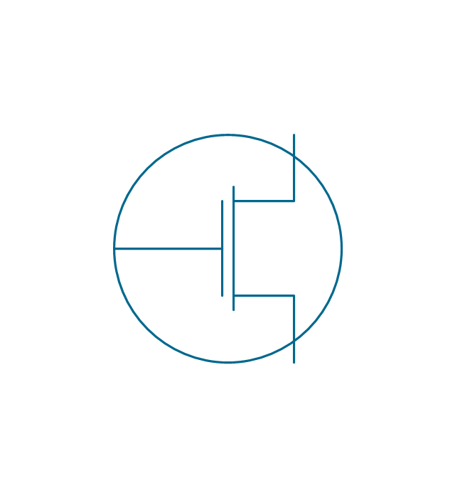
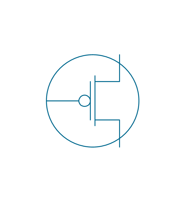
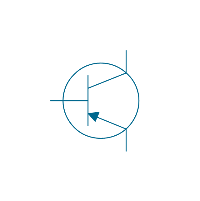
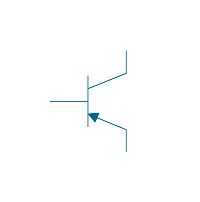
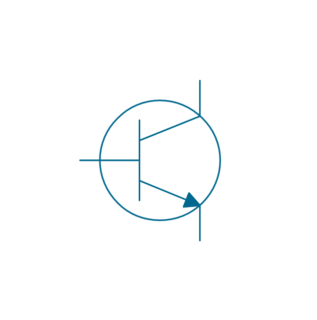
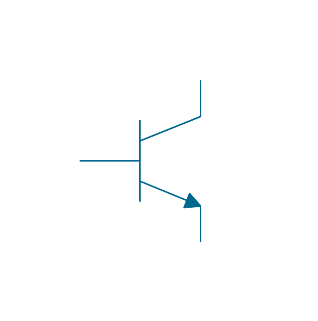
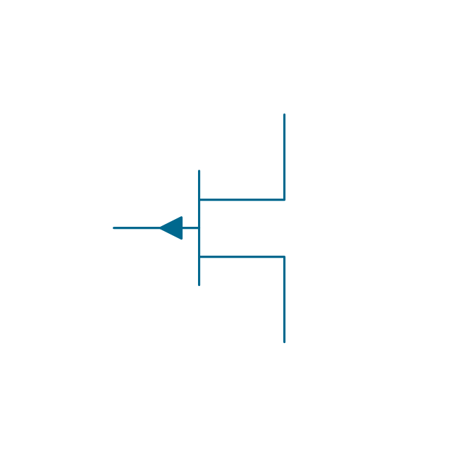
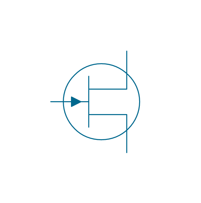
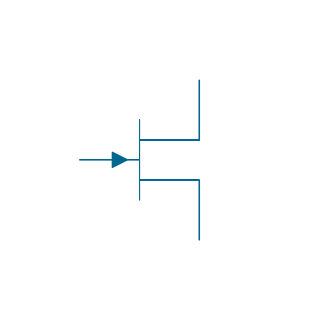
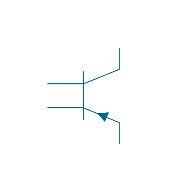
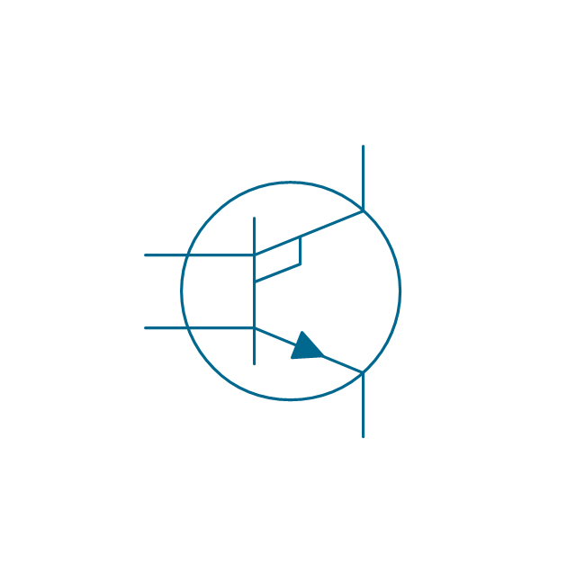
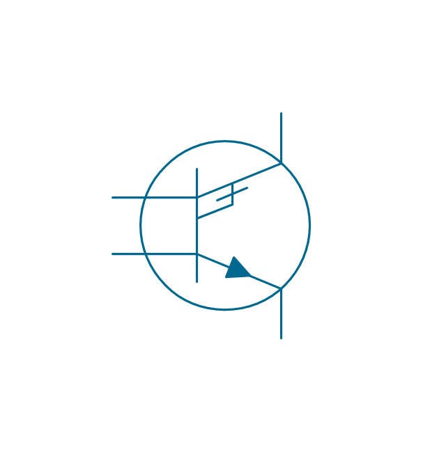
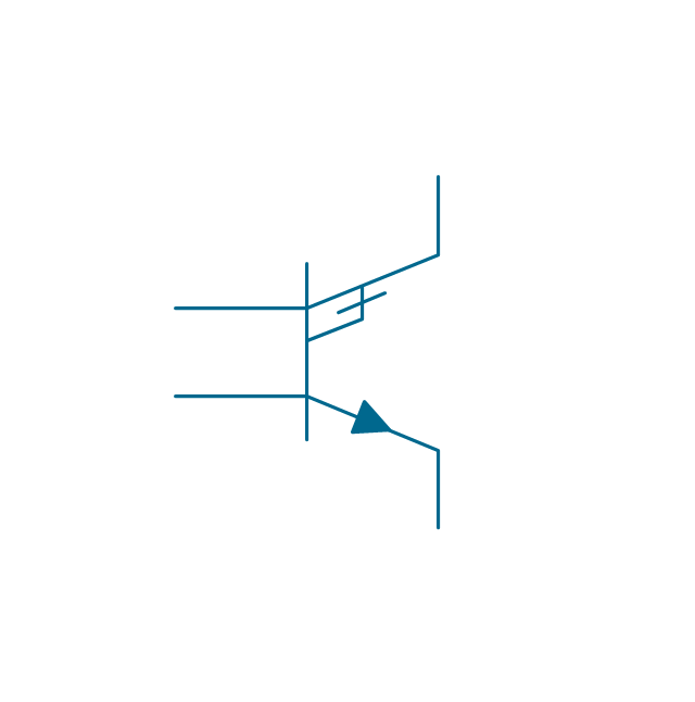
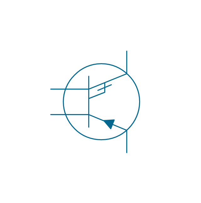
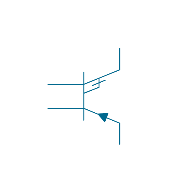
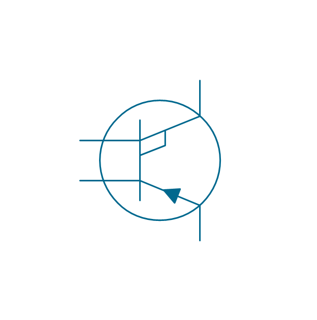
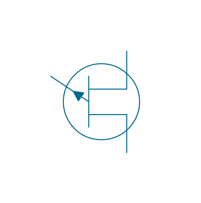
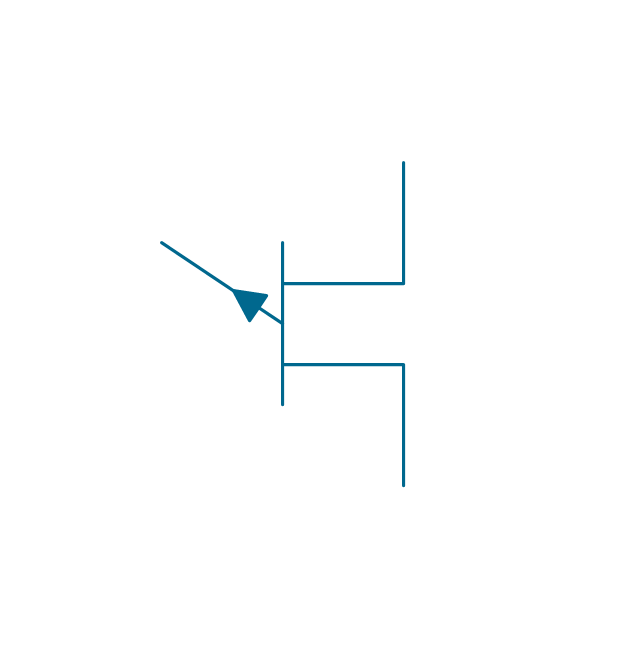
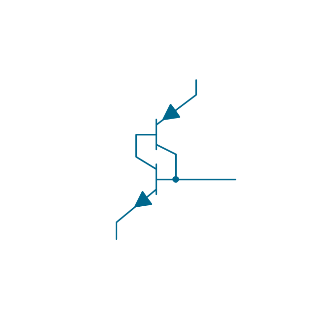
"A variety of symbols are used for the MOSFET. The basic design is generally a line for the channel with the source and drain leaving it at right angles and then bending back at right angles into the same direction as the channel. Sometimes three line segments are used for enhancement mode and a solid line for depletion mode. ... Another line is drawn parallel to the channel for the gate.
The "bulk" or "body" connection, if shown, is shown connected to the back of the channel with an arrow indicating PMOS or NMOS. Arrows always point from P to N, so an NMOS (N-channel in P-well or P-substrate) has the arrow pointing in (from the bulk to the channel). If the bulk is connected to the source (as is generally the case with discrete devices) it is sometimes angled to meet up with the source leaving the transistor. If the bulk is not shown (as is often the case in IC design as they are generally common bulk) an inversion symbol is sometimes used to indicate PMOS, alternatively an arrow on the source may be used in the same way as for bipolar transistors (out for nMOS, in for pMOS). ...
For the symbols in which the bulk, or body, terminal is shown, it is here shown internally connected to the source... This is a typical configuration, but by no means the only important configuration. In general, the MOSFET is a four-terminal device, and in integrated circuits many of the MOSFETs share a body connection, not necessarily connected to the source terminals of all the transistors." [MOSFET. Wikipedia]
The symbols example "Design elements - MOSFET" was drawn using the ConceptDraw PRO diagramming and vector drawing software extended with the Electrical Engineering solution from the Engineering area of ConceptDraw Solution Park.
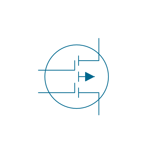
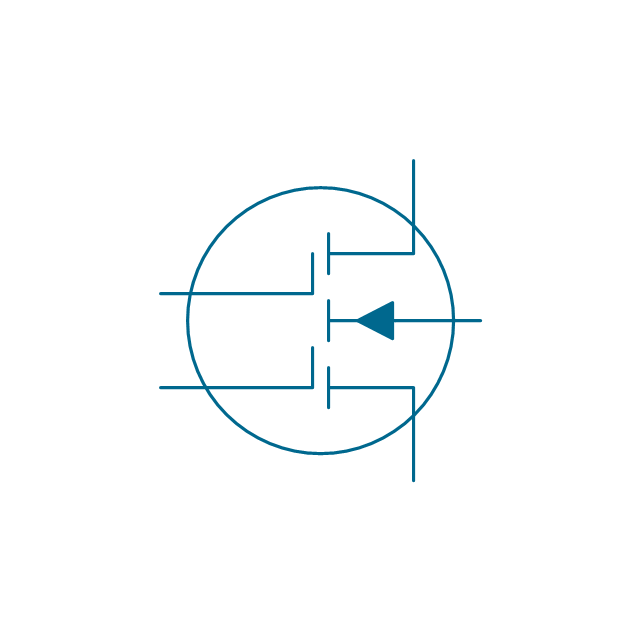
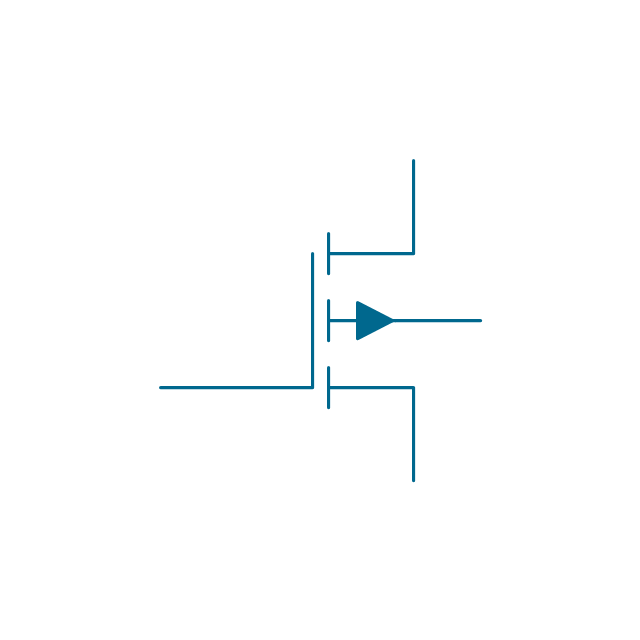
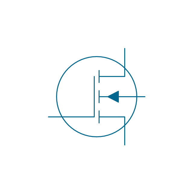
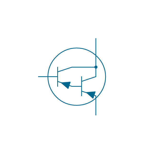
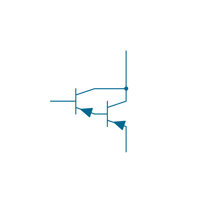
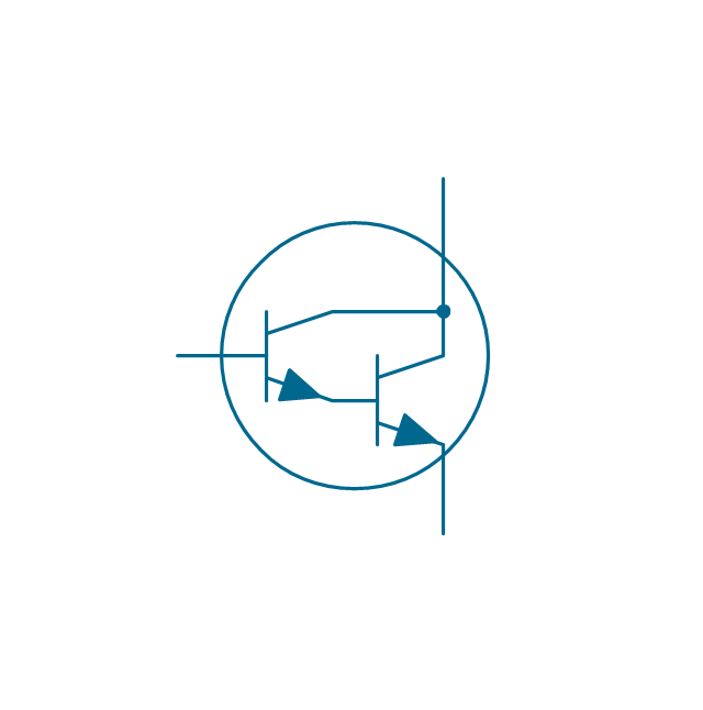
MOSFET symbols
The vector stencils library "Transistors" contains 30 symbols of transistors.
Use these shapes for drawing electronic schematics and circuit diagrams in the ConceptDraw PRO diagramming and vector drawing software extended with the Electrical Engineering solution from the Engineering area of ConceptDraw Solution Park.
www.conceptdraw.com/ solution-park/ engineering-electrical
Use these shapes for drawing electronic schematics and circuit diagrams in the ConceptDraw PRO diagramming and vector drawing software extended with the Electrical Engineering solution from the Engineering area of ConceptDraw Solution Park.
www.conceptdraw.com/ solution-park/ engineering-electrical
BJT, PNP, env
BJT, PNP
BJT, NPN, env
BJT, NPN
JFET, P, env

JFET, P
JFET, N, env
JFET, N
Transverse biased base, PNP, env

Transverse biased base, PNP
Transverse biased base, NPN, env

Transverse biased base, NPN

Ohmic, NPIN, env
Ohmic, NPIN

Ohmic, NPIP, env
Ohmic, NPIP
Ohmic, PNIN, env
Ohmic, PNIN
Ohmic, PNIP, env
Ohmic, PNIP

Unijunction FET, P, env
Unijunction FET, P
Unijunction FET, N, env

Unijunction FET, N

Darlington transistor, PNP, env
Darlington transistor, PNP
Darlington transistor, NPN, env
Darlington transistor, NPN

Transistor latch, env
Transistor latch
The vector stencils library "IGFET" contains 18 symbols of IGFET (insulated-gate field-effect transistor) elements for drawing electronic circuit diagrams.
"The metal–oxide–semiconductor field-effect transistor (MOSFET, MOS-FET, or MOS FET) is a transistor used for amplifying or switching electronic signals. Although the MOSFET is a four-terminal device with source (S), gate (G), drain (D), and body (B) terminals, the body (or substrate) of the MOSFET often is connected to the source terminal, making it a three-terminal device like other field-effect transistors. Because these two terminals are normally connected to each other (short-circuited) internally, only three terminals appear in electrical diagrams. The MOSFET is by far the most common transistor in both digital and analog circuits, though the bipolar junction transistor was at one time much more common. ...
An insulated-gate field-effect transistor or IGFET is a related term almost synonymous with MOSFET. The term may be more inclusive, since many "MOSFETs" use a gate that is not metal, and a gate insulator that is not oxide. Another synonym is MISFET for metal–insulator–semiconductor FET." [MOSFET
From Wikipedia]
The symbols example "Design elements - IGFET" was drawn using the ConceptDraw PRO diagramming and vector drawing software extended with the Electrical Engineering solution from the Engineering area of ConceptDraw Solution Park.
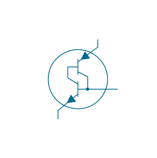
IGFET elements

Electrical Symbols — IGFET

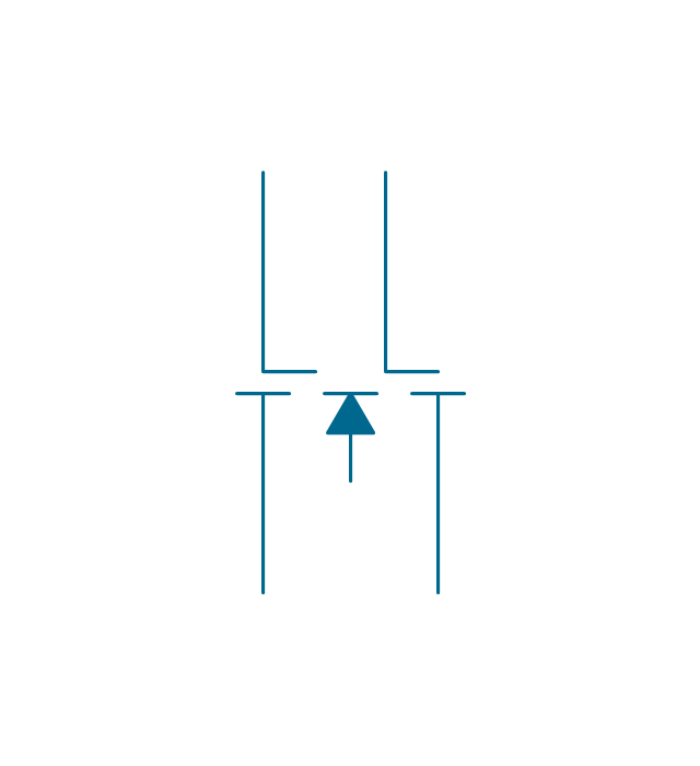
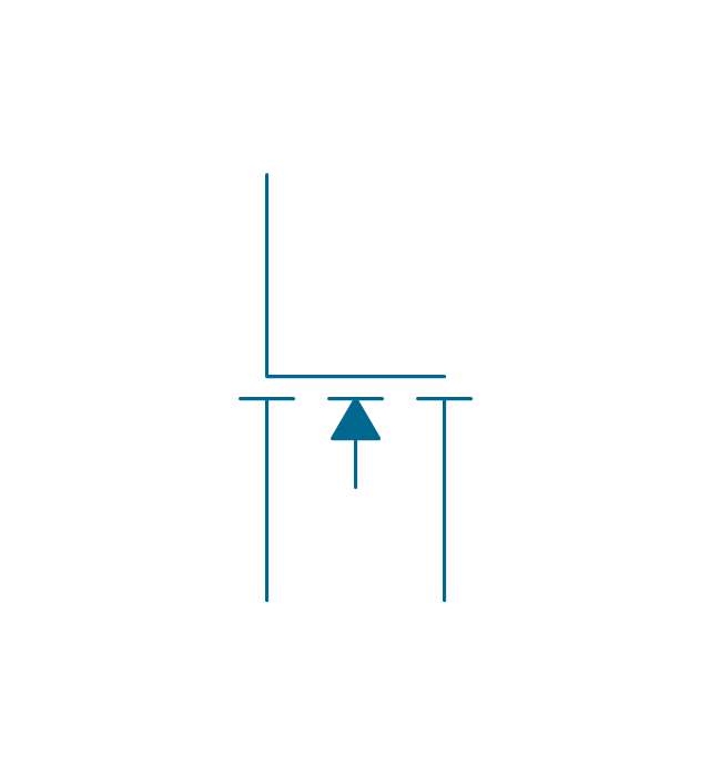
Electrical Symbols — MOSFET

The vector stencils library "MOSFET" contains 18 symbols of MOSFET (metal–oxide–semiconductor field-effect transistor) elements.
Use these shapes for drawing electronic circuits diagrams in the ConceptDraw PRO diagramming and vector drawing software extended with the Electrical Engineering solution from the Engineering area of ConceptDraw Solution Park.
www.conceptdraw.com/ solution-park/ engineering-electrical
Use these shapes for drawing electronic circuits diagrams in the ConceptDraw PRO diagramming and vector drawing software extended with the Electrical Engineering solution from the Engineering area of ConceptDraw Solution Park.
www.conceptdraw.com/ solution-park/ engineering-electrical
MOSFET, P, dep, 2 gates, env
MOSFET, P, dep, 2 gates
MOSFET, N, dep, 2 gates, env
MOSFET, N, dep, 2 gates
MOSFET, P, dep, 1 gate, env
MOSFET, P, dep, 1 gate
MOSFET, N, dep, 1 gate, env
MOSFET, N, dep, 1 gate
MOSFET, P, enh, 2 gates, env
MOSFET, P, enh, 2 gates
MOSFET, N, enh, 2 gates, env
MOSFET, N, enh, 2 gates
MOSFET, P, enh, 1 gate, env
MOSFET, P, enh, 1 gate
MOSFET, N, enh, 1 gate, env
MOSFET, N, enh, 1 gate
MOSFET, P, enh, Sedra
MOSFET, N, enh, Sedra
The vector stencils library "MOSFET" contains 18 symbols of MOSFET (metal–oxide–semiconductor field-effect transistor) elements for drawing electronic circuits diagrams.
"A variety of symbols are used for the MOSFET. The basic design is generally a line for the channel with the source and drain leaving it at right angles and then bending back at right angles into the same direction as the channel. Sometimes three line segments are used for enhancement mode and a solid line for depletion mode. ... Another line is drawn parallel to the channel for the gate.
The "bulk" or "body" connection, if shown, is shown connected to the back of the channel with an arrow indicating PMOS or NMOS. Arrows always point from P to N, so an NMOS (N-channel in P-well or P-substrate) has the arrow pointing in (from the bulk to the channel). If the bulk is connected to the source (as is generally the case with discrete devices) it is sometimes angled to meet up with the source leaving the transistor. If the bulk is not shown (as is often the case in IC design as they are generally common bulk) an inversion symbol is sometimes used to indicate PMOS, alternatively an arrow on the source may be used in the same way as for bipolar transistors (out for nMOS, in for pMOS). ...
For the symbols in which the bulk, or body, terminal is shown, it is here shown internally connected to the source... This is a typical configuration, but by no means the only important configuration. In general, the MOSFET is a four-terminal device, and in integrated circuits many of the MOSFETs share a body connection, not necessarily connected to the source terminals of all the transistors." [MOSFET. Wikipedia]
The symbols example "Design elements - MOSFET" was drawn using the ConceptDraw PRO diagramming and vector drawing software extended with the Electrical Engineering solution from the Engineering area of ConceptDraw Solution Park.
MOSFET symbols
Electrical Symbols — Transistors

The vector stencils library "Logic gate diagram" contains 17 element symbols for drawing the logic gate diagrams.
"To build a functionally complete logic system, relays, valves (vacuum tubes), or transistors can be used. The simplest family of logic gates using bipolar transistors is called resistor-transistor logic (RTL). Unlike simple diode logic gates (which do not have a gain element), RTL gates can be cascaded indefinitely to produce more complex logic functions. RTL gates were used in early integrated circuits. For higher speed and better density, the resistors used in RTL were replaced by diodes resulting in diode-transistor logic (DTL). Transistor-transistor logic (TTL) then supplanted DTL. As integrated circuits became more complex, bipolar transistors were replaced with smaller field-effect transistors (MOSFETs); see PMOS and NMOS. To reduce power consumption still further, most contemporary chip implementations of digital systems now use CMOS logic. CMOS uses complementary (both n-channel and p-channel) MOSFET devices to achieve a high speed with low power dissipation." [Logic gate. Wikipedia]
The symbols example "Design elements - Logic gate diagram" was drawn using the ConceptDraw PRO diagramming and vector drawing software extended with the Electrical Engineering solution from the Engineering area of ConceptDraw Solution Park.
Logic gate symbols
CAD Drawing Software for Making Mechanic Diagram and Electrical Diagram Architectural Designs


Electrical Symbols — Semiconductor

Process Flowchart


- Symbol In P
- Drawing P
- Microsoft Visio P
- Design elements - MOSFET | Design elements - Transistors | Design ...
- Electrical Symbols — MOSFET | Electrical Symbols , Electrical ...
- Types And Symbols Of Field Effect Transistor
- Electrical Symbols — MOSFET | Design elements - Transistors ...
- Reduce Valve P
- Design elements - Transistors | Design elements - MOSFET | Design ...
- Design elements - MOSFET | Design elements - Transistors ...
- Circuit Diagram Using P
- Design elements - MOSFET | Design elements - Transistors ...
- Electrical Symbols — MOSFET | Electrical Symbols — Transistors ...
- Design elements - Transistors | Transistors - Vector stencils library ...
- Electrical Symbols — MOSFET | Cisco Multimedia, Voice, Phone ...
- Electrical Symbols — Transistors | Transistors - Vector stencils ...
- Baseball Diagram – Baseball Field – Corner View – Sample ...
- Center Field In Baseball
- Process P