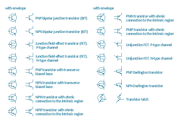
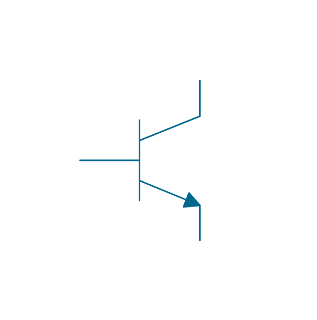
The vector stencils library "Transistors" contains 30 symbols of transistors drawing electronic schematics and circuit diagrams.
"A transistor is a semiconductor device used to amplify and switch electronic signals and electrical power. It is composed of semiconductor material with at least three terminals for connection to an external circuit. A voltage or current applied to one pair of the transistor's terminals changes the current through another pair of terminals. Because the controlled (output) power can be higher than the controlling (input) power, a transistor can amplify a signal. Today, some transistors are packaged individually, but many more are found embedded in integrated circuits.
The transistor is the fundamental building block of modern electronic devices, and is ubiquitous in modern electronic systems. ...
Transistors are categorized by:
(1) Semiconductor material...: the metalloids germanium ... and silicon ... in amorphous, polycrystalline and monocrystalline form; the compounds gallium arsenide ... and silicon carbide ..., the alloy silicon-germanium ..., the allotrope of carbon graphene ...
(2) Structure: BJT, JFET, IGFET (MOSFET), insulated-gate bipolar transistor, "other types"
(3) Electrical polarity (positive and negative): n–p–n, p–n–p (BJTs); n-channel, p-channel (FETs)
(4) Maximum power rating: low, medium, high
(5) Maximum operating frequency: low, medium, high, radio (RF), microwave frequency...
(6) Application: switch, general purpose, audio, high voltage, super-beta, matched pair
(7) Physical packaging: through-hole metal, through-hole plastic, surface mount, ball grid array, power modules...
(8) Amplification factor..." [Transistor. Wikipedia]
The shapes example "Design elements - Transistors" was drawn using the ConceptDraw PRO diagramming and vector drawing software extended with the Electrical Engineering solution from the Engineering area of ConceptDraw Solution Park.
Transistor symbols
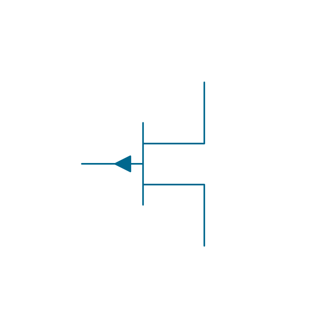
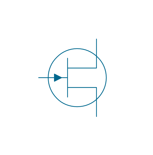
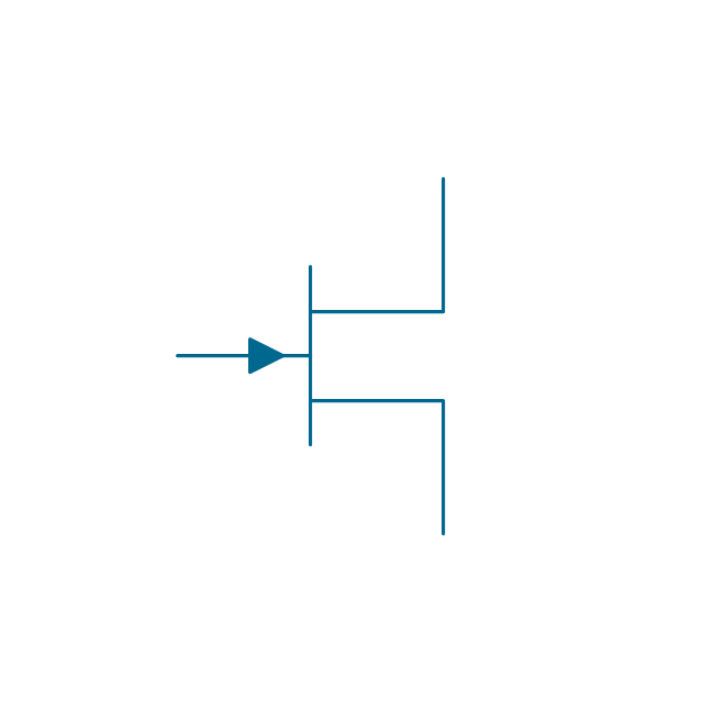
The vector stencils library "IGFET" contains 18 symbols of IGFET (insulated-gate field-effect transistor) elements for drawing electronic circuit diagrams.
"The metal–oxide–semiconductor field-effect transistor (MOSFET, MOS-FET, or MOS FET) is a transistor used for amplifying or switching electronic signals. Although the MOSFET is a four-terminal device with source (S), gate (G), drain (D), and body (B) terminals, the body (or substrate) of the MOSFET often is connected to the source terminal, making it a three-terminal device like other field-effect transistors. Because these two terminals are normally connected to each other (short-circuited) internally, only three terminals appear in electrical diagrams. The MOSFET is by far the most common transistor in both digital and analog circuits, though the bipolar junction transistor was at one time much more common. ...
An insulated-gate field-effect transistor or IGFET is a related term almost synonymous with MOSFET. The term may be more inclusive, since many "MOSFETs" use a gate that is not metal, and a gate insulator that is not oxide. Another synonym is MISFET for metal–insulator–semiconductor FET." [MOSFET
From Wikipedia]
The symbols example "Design elements - IGFET" was drawn using the ConceptDraw PRO diagramming and vector drawing software extended with the Electrical Engineering solution from the Engineering area of ConceptDraw Solution Park.
IGFET elements

The vector stencils library "Transistors" contains 30 symbols of transistors.
Use these shapes for drawing electronic schematics and circuit diagrams in the ConceptDraw PRO diagramming and vector drawing software extended with the Electrical Engineering solution from the Engineering area of ConceptDraw Solution Park.
www.conceptdraw.com/ solution-park/ engineering-electrical
Use these shapes for drawing electronic schematics and circuit diagrams in the ConceptDraw PRO diagramming and vector drawing software extended with the Electrical Engineering solution from the Engineering area of ConceptDraw Solution Park.
www.conceptdraw.com/ solution-park/ engineering-electrical
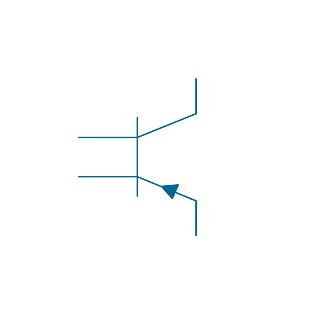
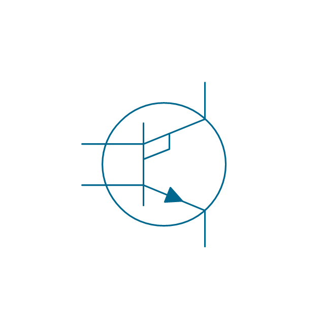
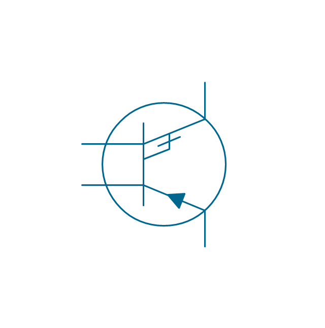
BJT, PNP, env
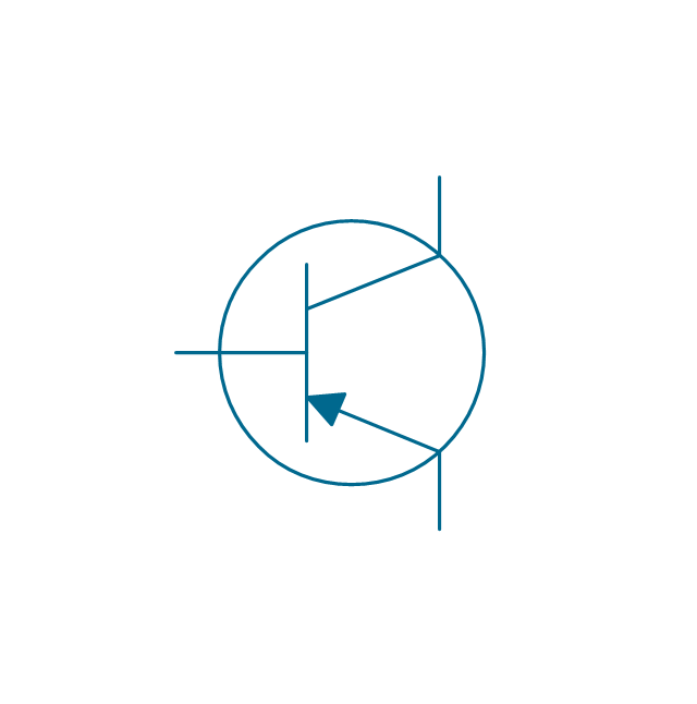
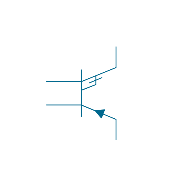
BJT, PNP
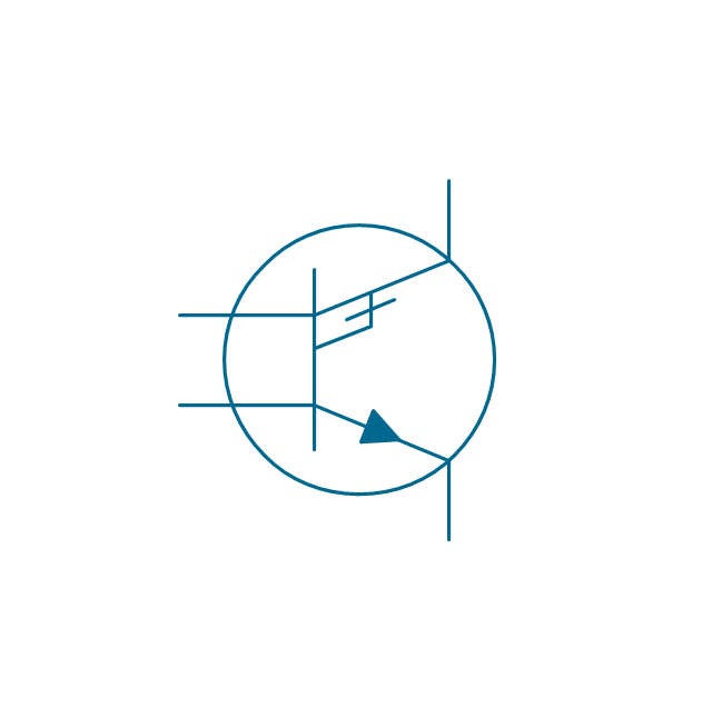
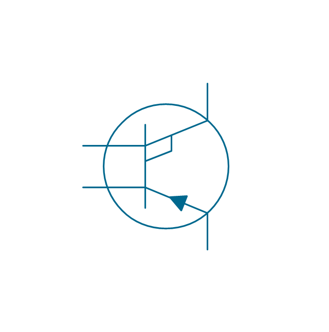
BJT, NPN, env
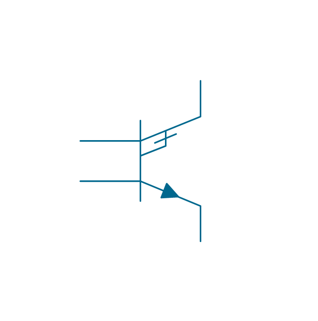
BJT, NPN
JFET, P, env

JFET, P
JFET, N, env
JFET, N
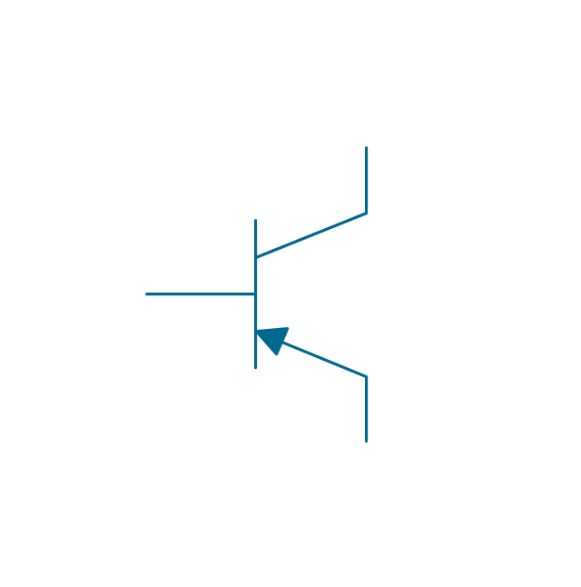
Transverse biased base, PNP, env

Transverse biased base, PNP
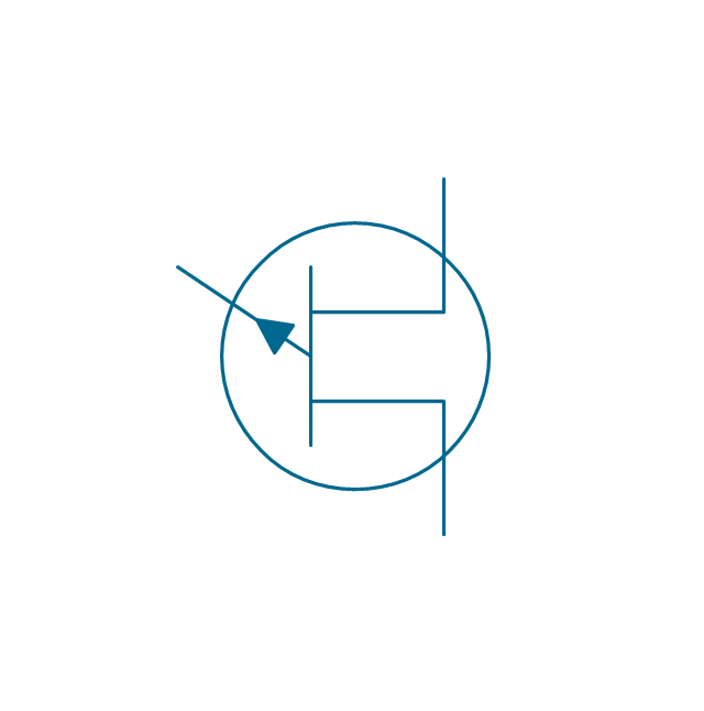
Transverse biased base, NPN, env

Transverse biased base, NPN

Ohmic, NPIN, env
Ohmic, NPIN

Ohmic, NPIP, env
Ohmic, NPIP
Ohmic, PNIN, env
Ohmic, PNIN
Ohmic, PNIP, env
Ohmic, PNIP

Unijunction FET, P, env
Unijunction FET, P
Unijunction FET, N, env

Unijunction FET, N

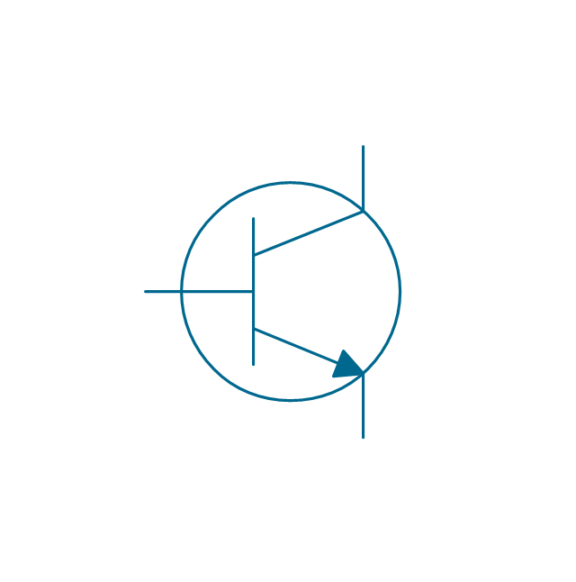
Darlington transistor, PNP, env
Darlington transistor, PNP
Darlington transistor, NPN, env
Darlington transistor, NPN

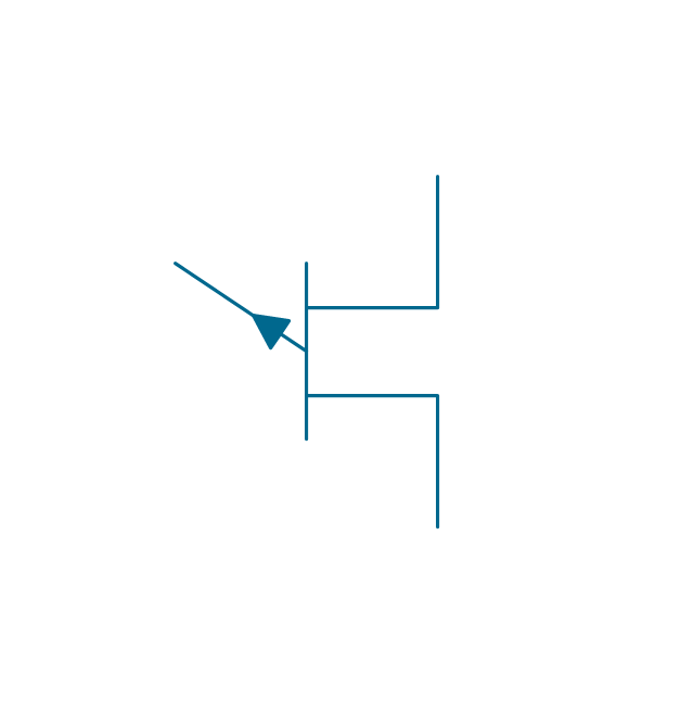
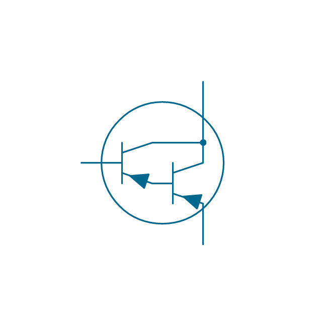
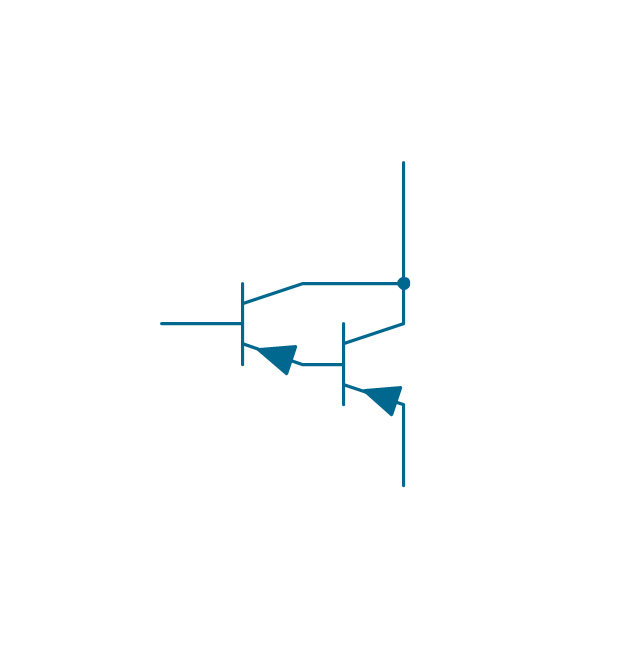
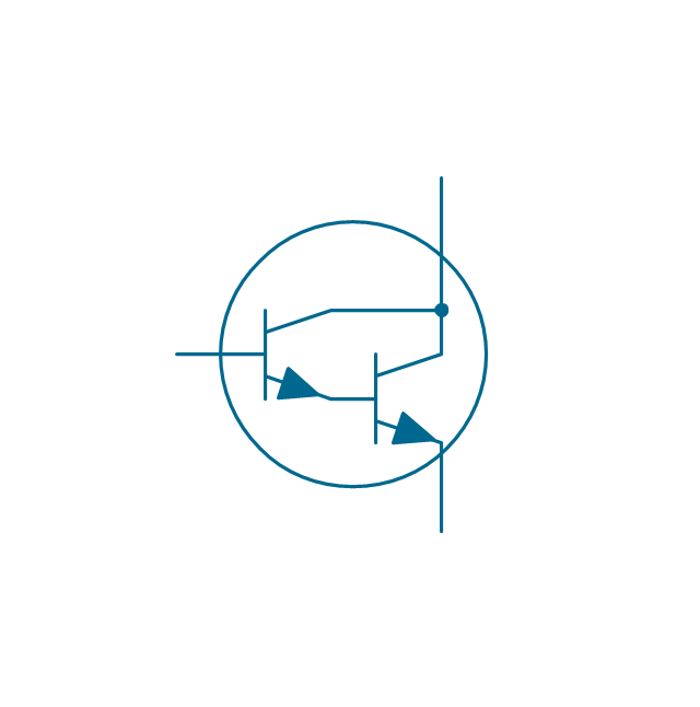
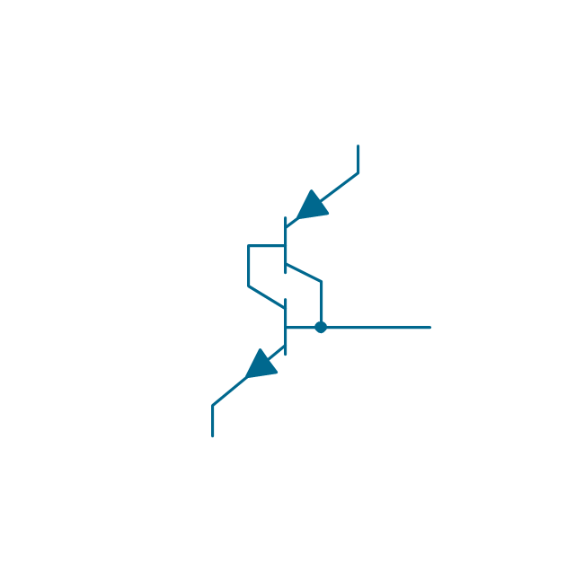
Transistor latch, env
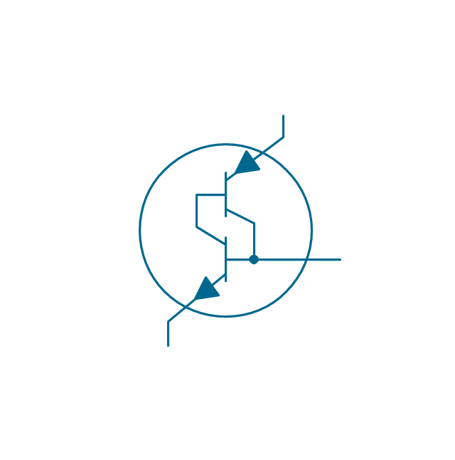
Transistor latch
- Transistors - Vector stencils library | Design elements - Transistors ...
- Design elements - Transistors | Design elements - IGFET ...
- Symbol Of Switches And Rating Of Electrical
- Transistor Types And Application
- Design elements - MOSFET | Design elements - Transistors | Sales ...
- Electrical Diagram Symbols | Design elements - Semiconductor ...
- Symbol Of Semiconductor
- Symbol Of The Elements Of Electronic
- Electrical Power Symbols
- How To use House Electrical Plan Software | Making Mechanical ...
- Electrical Diagram Symbols | Design elements - Switches | How To ...
- Draw An Electric Circuit With Symbol
- Electrical Drawing Software | How To use House Electrical Plan ...
- Design elements - HVAC ductwork
- Electrical Symbols And Frequency
- HVAC controls - Vector stencils library
- Design elements - Transistors | Design elements - Semiconductors ...
- Design elements - Composite assemblies | Design elements ...
- Control devices - Vector stencils library | Design elements ...
- How To use Electrical and Telecom Plan Software | Circuits and ...