 Electrical Engineering
This solution extends ConceptDraw PRO v.9.5 (or later) with electrical engineering samples, electrical schematic symbols, electrical diagram symbols, templates and libraries of design elements, to help you design electrical schematics, digital and analog
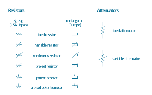
The vector stencils library "Resistors" contains 14 element symbols of resistors for drawing electronic schematics, circuit diagrams and electrical drawings.
"A resistor is a passive two-terminal electrical component that implements electrical resistance as a circuit element. Resistors act to reduce current flow, and, at the same time, act to lower voltage levels within circuits. Resistors may have fixed resistances or variable resistances, such as those found in thermistors, varistors, trimmers, photoresistors and potentiometers.
The current through a resistor is in direct proportion to the voltage across the resistor's terminals. This relationship is represented by Ohm's law ...
Resistors are common elements of electrical networks and electronic circuits and are ubiquitous in electronic equipment. Practical resistors can be composed of various compounds and films, as well as resistance wires (wire made of a high-resistivity alloy, such as nickel-chrome). Resistors are also implemented within integrated circuits, particularly analog devices, and can also be integrated into hybrid and printed circuits." [Resistor. Wikipedia]
The shapes example "Design elements - Resistors" was drawn using the ConceptDraw PRO diagramming and vector drawing software extended with the Electrical Engineering solution from the Engineering area of ConceptDraw Solution Park.
Resistor symbols
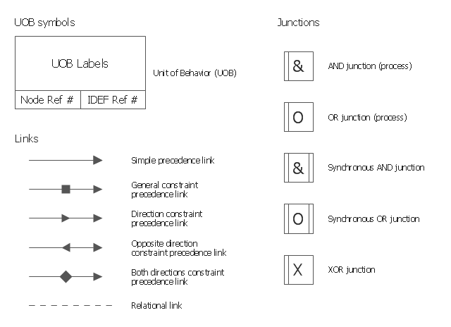
The vector stencils library "IDEF3 process schematic symbols" contains 12 shapes: unit of behavior (UOB), links, junctions, .
Use it to design your IDEF3 process schematic diagrams.
"Process schematics tend to be the most familiar and broadly used component of the IDEF3 method. These schematics provide a visualization mechanism for processcentered descriptions of a scenario. The graphical elements that comprise process schematics include Unit of Behavior (UOB) boxes, precedence links, junctions, referents, and notes. The building blocks here are:
- Unit of Behavior (UOB) boxes.
- Links: Links are the glue that connect UOB boxes to form representations of dynamic processes.
- Simple Precedence Links: Precedence links express temporal precedence relations between instances of one UOB and those of another.
- Activation Plots: Activation plots are used to represent activations.
- Dashed Links: Dashed links carry no predefined semantics.
- Link Numbers: All links have an elaboration and unique link numbers.
Activation Semantics for Nonbranching Process Schematics.
- Junctions: Junctions in IDEF3 provide a mechanism to specify the logic of process branching.
- UOB Decompositions: Elaborations capture and structure detailed knowledge about processes.
- UOB Reference Numbering Scheme: A UOB box number is assigned to each UOB box in an IDEF3 Process Description.
- Partial Descriptions: UOB boxes are joined together by links. Because of the description capture focus of IDEF3, it is possible to conceive of UOBs without links to other parts of an IDEF3 schematic.
- Referents: Referents enhance understanding, provide additional meaning, and simplify the construction (i.e., minimize clutter) of both process schematics and object schematics." [IDEF3. Wikipedia]
The shapes example "Design elements - IDEF3 process schematic symbols" was created using the ConceptDraw PRO diagramming and vector drawing software extended with the solution "IDEF Business Process Diagrams" from the area "Business Processes" of ConceptDraw Solution Park.
IDEF3 business process diagram
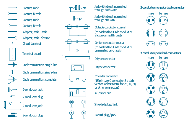
The vector stencils library "Terminals and connectors" contains 43 element symbols of terminals, connectors, plugs, polarized connectors, jacks, coaxial cables, and conductors.
Use it for drawing the wiring diagrams, electrical layouts, electronic schematics, and circuit diagrams.
"An electrical connector is an electro-mechanical device for joining electrical circuits as an interface using a mechanical assembly. Connectors consist of plugs (male-ended) and jacks (female-ended). The connection may be temporary, as for portable equipment, require a tool for assembly and removal, or serve as a permanent electrical joint between two wires or devices. An adapter can be used to effectively bring together dissimilar connectors.
There are hundreds of types of electrical connectors. Connectors may join two lengths of flexible copper wire or cable, or connect a wire or cable or optical interface to an electrical terminal.
In computing, an electrical connector can also be known as a physical interface... Cable glands, known as cable connectors in the US, connect wires to devices mechanically rather than electrically and are distinct from quick-disconnects performing the latter." [Electrical connector. Wikipedia]
"A terminal is the point at which a conductor from an electrical component, device or network comes to an end and provides a point of connection to external circuits. A terminal may simply be the end of a wire or it may be fitted with a connector or fastener. In network analysis, terminal means a point at which connections can be made to a network in theory and does not necessarily refer to any real physical object. In this context, especially in older documents, it is sometimes called a "pole".
The connection may be temporary, as seen in portable equipment, may require a tool for assembly and removal, or may be a permanent electrical joint between two wires or devices.
All electric cell have two terminals. The first is the positive terminal and the second is the negative terminal. The positive terminal looks like a metal cap and the negative terminal looks like a metal disc. The current flows from the positive terminal, and out through the negative terminal, replicative of current flow (positive (+) to negative (-) flow)." [Terminal (electronics). Wikipedia]
The shapes example "Design elements - Terminals and connectors" was drawn using the ConceptDraw PRO diagramming and vector drawing software extended with the Electrical Engineering solution from the Engineering area of ConceptDraw Solution Park.
Terminal and connector symbols
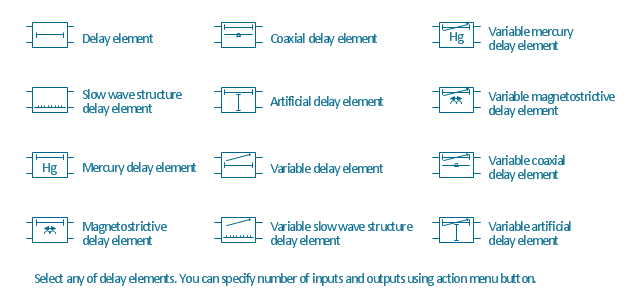
The vector stencils library "Delay elements" contains 12 symbols of delay elements for drawing electrical schematics and electronic circuit diagrams.
"An analog delay line is a network of electrical components connected in series, where each individual element creates a time difference or phase change between its input signal and its output signal. It operates on analog signals whose amplitude varies continuously. An example is a bucket-brigade device. Other types of delay line include acoustic, magnetostrictive, and surface acoustic wave devices. A series of RC networks can be cascaded to form a delay. A long transmission line can also provide a delay element. The delay time of an analog delay line may be only a few nanoseconds or several milliseconds, limited by the practical size of the physical medium used to delay the signal and the propagation speed of impulses in the medium." [Analog delay line. Wikipedia]
The symbols example "Design elements - Delay elements" was drawn using the ConceptDraw PRO diagramming and vector drawing software extended with the Electrical Engineering solution from the Engineering area of ConceptDraw Solution Park.
Delay element symbols
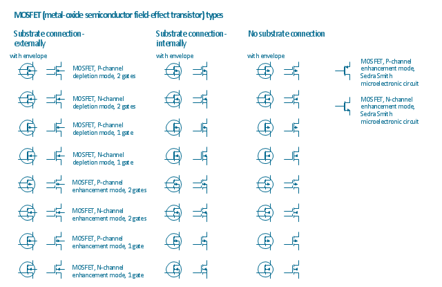
The vector stencils library "MOSFET" contains 18 symbols of MOSFET (metal–oxide–semiconductor field-effect transistor) elements for drawing electronic circuits diagrams.
"A variety of symbols are used for the MOSFET. The basic design is generally a line for the channel with the source and drain leaving it at right angles and then bending back at right angles into the same direction as the channel. Sometimes three line segments are used for enhancement mode and a solid line for depletion mode. ... Another line is drawn parallel to the channel for the gate.
The "bulk" or "body" connection, if shown, is shown connected to the back of the channel with an arrow indicating PMOS or NMOS. Arrows always point from P to N, so an NMOS (N-channel in P-well or P-substrate) has the arrow pointing in (from the bulk to the channel). If the bulk is connected to the source (as is generally the case with discrete devices) it is sometimes angled to meet up with the source leaving the transistor. If the bulk is not shown (as is often the case in IC design as they are generally common bulk) an inversion symbol is sometimes used to indicate PMOS, alternatively an arrow on the source may be used in the same way as for bipolar transistors (out for nMOS, in for pMOS). ...
For the symbols in which the bulk, or body, terminal is shown, it is here shown internally connected to the source... This is a typical configuration, but by no means the only important configuration. In general, the MOSFET is a four-terminal device, and in integrated circuits many of the MOSFETs share a body connection, not necessarily connected to the source terminals of all the transistors." [MOSFET. Wikipedia]
The symbols example "Design elements - MOSFET" was drawn using the ConceptDraw PRO diagramming and vector drawing software extended with the Electrical Engineering solution from the Engineering area of ConceptDraw Solution Park.
MOSFET symbols
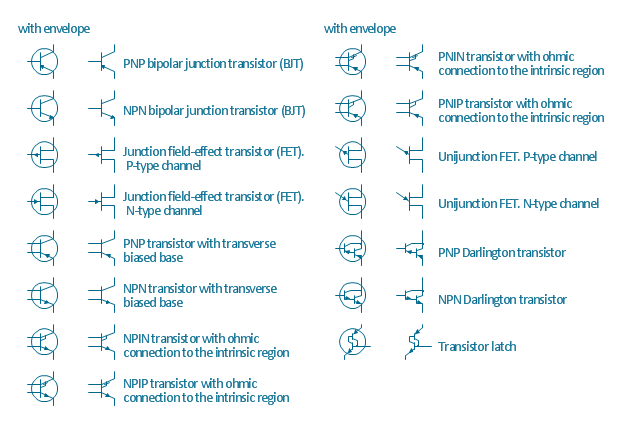
The vector stencils library "Transistors" contains 30 symbols of transistors drawing electronic schematics and circuit diagrams.
"A transistor is a semiconductor device used to amplify and switch electronic signals and electrical power. It is composed of semiconductor material with at least three terminals for connection to an external circuit. A voltage or current applied to one pair of the transistor's terminals changes the current through another pair of terminals. Because the controlled (output) power can be higher than the controlling (input) power, a transistor can amplify a signal. Today, some transistors are packaged individually, but many more are found embedded in integrated circuits.
The transistor is the fundamental building block of modern electronic devices, and is ubiquitous in modern electronic systems. ...
Transistors are categorized by:
(1) Semiconductor material...: the metalloids germanium ... and silicon ... in amorphous, polycrystalline and monocrystalline form; the compounds gallium arsenide ... and silicon carbide ..., the alloy silicon-germanium ..., the allotrope of carbon graphene ...
(2) Structure: BJT, JFET, IGFET (MOSFET), insulated-gate bipolar transistor, "other types"
(3) Electrical polarity (positive and negative): n–p–n, p–n–p (BJTs); n-channel, p-channel (FETs)
(4) Maximum power rating: low, medium, high
(5) Maximum operating frequency: low, medium, high, radio (RF), microwave frequency...
(6) Application: switch, general purpose, audio, high voltage, super-beta, matched pair
(7) Physical packaging: through-hole metal, through-hole plastic, surface mount, ball grid array, power modules...
(8) Amplification factor..." [Transistor. Wikipedia]
The shapes example "Design elements - Transistors" was drawn using the ConceptDraw PRO diagramming and vector drawing software extended with the Electrical Engineering solution from the Engineering area of ConceptDraw Solution Park.
Transistor symbols
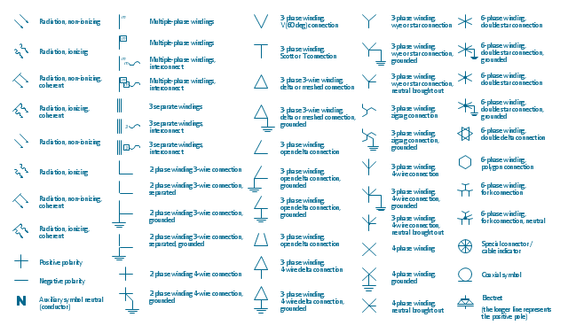
The vector stencils library "Qualifying" contains 56 qualifying symbols of radiation, polarity, phase, windings, wire, ground, connection, connector, coaxial, electret.
Use these signs to annotate or specify characteristics of objects in electrical drawings, electronic schematics, circuit diagrams, electromechanical drawings, and wiring diagrams, cabling layout diagrams.
"An electrical drawing, is a type of technical drawing that shows information about power, lighting, and communication for an engineering or architectural project. Any electrical working drawing consists of "lines, symbols, dimensions, and notations to accurately convey an engineering's design to the workers, who install the electrical system on the job".
A complete set of working drawings for the average electrical system in large projects usually consists of:
(1) A plot plan showing the building's location and outside electrical wiring.
(2) Floor plans showing the location of electrical systems on every floor.
(3) Power-riser diagrams showing panel boards.
(4) Control wiring diagrams.
(5) Schedules and other information in combination with construction drawings.
Electrical drafters prepare wiring and layout diagrams used by workers who erect, install, and repair electrical equipment and wiring in communication centers, power plants, electrical distribution systems, and buildings." [Electrical drawing. Wikipedia]
The signs example "Design elements - Qualifying" was drawn using the ConceptDraw PRO diagramming and vector drawing software extended with the Electrical Engineering solution from the Engineering area of ConceptDraw Solution Park.
Qualifying symbols
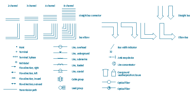
The vector stencils library "Transmission paths" contains 43 symbols of power transmission paths, electronic circuits, bus connectors and elbows, terminals, junctions, and concentrators.
Use it to annotate electrical diagrams, electronic schematics and circuit diagrams.
"A physical medium in data communications is the transmission path over which a signal propagates.
Many transmission media are used as communications channel.
For telecommunications purposes in the United States, Federal Standard 1037C, transmission media are classified as one of the following:
(1) Guided (or bounded) - waves are guided along a solid medium such as a transmission line.
(2) Wireless (or unguided) - transmission and reception are achieved by means of an antenna.
One of the most common physical medias used in networking is copper wire. Copper wire to carry signals to long distances using relatively low amounts of power. The unshielded twisted pair (UTP) is eight strands of copper wire, organized into four pairs.
Another example of a physical medium is optical fiber, which has emerged as the most commonly used transmission medium for long-distance communications. Optical fiber is a thin strand of glass that guides light along its length.
Multimode and single mode are two types of commonly used optical fiber. Multimode fiber uses LEDs as the light source and can carry signals over shorter distances, about 2 kilometers. Single mode can carry signals over distances of tens of miles.
Wireless media may carry surface waves or skywaves, either longitudinally or transversely, and are so classified.
In both communications, communication is in the form of electromagnetic waves. With guided transmission media, the waves are guided along a physical path; examples of guided media include phone lines, twisted pair cables, coaxial cables, and optical fibers. Unguided transmission media are methods that allow the transmission of data without the use of physical means to define the path it takes. Examples of this include microwave, radio or infrared. Unguided media provide a means for transmitting electromagnetic waves but do not guide them; examples are propagation through air, vacuum and seawater.
The term direct link is used to refer to the transmission path between two devices in which signals propagate directly from transmitters to receivers with no intermediate devices, other than amplifiers or repeaters used to increase signal strength. This term can apply to both guided and unguided media.
A transmission may be simplex, half-duplex, or full-duplex.
In simplex transmission, signals are transmitted in only one direction; one station is a transmitter and the other is the receiver. In the half-duplex operation, both stations may transmit, but only one at a time. In full duplex operation, both stations may transmit simultaneously. In the latter case, the medium is carrying signals in both directions at same time." [Transmission medium. Wikipedia]
The shapes example "Design elements - Transmission paths" was drawn using the ConceptDraw PRO diagramming and vector drawing software extended with the Electrical Engineering solution from the Engineering area of ConceptDraw Solution Park.
Transmission path symbols
- Electrical Drawing Software and Electrical Symbols | Complex ...
- The Symbol For Circuit Breaker Used In Wiring Circuit Diagram
- Electrical Symbols , Electrical Diagram Symbols | How To use House ...
- Electrical Symbols , Electrical Diagram Symbols | Electrical Drawing ...
- Electrical Symbols — Transformers and Windings | Electrical ...
- Electrical Diagram Software | Bipolar current mirror - Circuit diagram ...
- Electrical Engineering | Bipolar current mirror - Circuit diagram ...
- Mechanical Drawing Symbols | Process Flow Diagram Symbols ...
- Home Theater Amplifier Circuit Diagram With Volume Control In
- Amplifier Circuit Schematics
- Schematic Symbols Of Valves
- Electrical circuits - Vector stencils library | Electrical Symbols ...
- Electrical Symbols , Electrical Diagram Symbols | Electrical Symbols ...
- Circuit diagram - EL 34 schematics | Electrical Symbols , Electrical ...
- Electrical Symbols , Electrical Diagram Symbols | Electrical Symbols ...
- Electromechanical Device Schematics And Electronic Circuit
- Electrical Symbols — Logic Gate Diagram
- Junction Amplifier Schematic
- Electrical Symbols , Electrical Diagram Symbols | How To use House ...