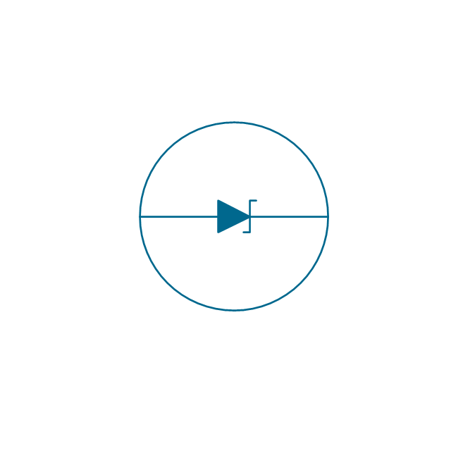
The vector stencils library "Semiconductor diodes" contains 24 symbols of semiconductor diodes for drawing electronic schematics and circuit diagrams.
"In electronics, a diode is a two-terminal electronic component with asymmetric conductance; it has low (ideally zero) resistance to current in one direction, and high (ideally infinite) resistance in the other. A semiconductor diode, the most common type today, is a crystalline piece of semiconductor material with a p–n junction connected to two electrical terminals. A vacuum tube diode has two electrodes, a plate (anode) and a heated cathode. Semiconductor diodes were the first semiconductor electronic devices. ...
Today, most diodes are made of silicon, but other semiconductors such as selenium or germanium are sometimes used." [Diode. Wikipedia]
The shapes example "Design elements - Semiconductor diodes" was drawn using the ConceptDraw PRO diagramming and vector drawing software extended with the Electrical Engineering solution from the Engineering area of ConceptDraw Solution Park.
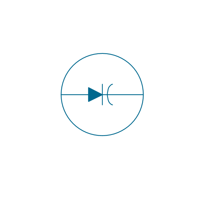
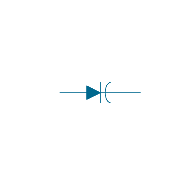
Semiconductor diode symbols

The vector stencils library "Semiconductor diodes" contains 24 symbols of semiconductor diodes.
Use these shapes for drawing electronic schematics and circuit diagrams in the ConceptDraw PRO diagramming and vector drawing software extended with the Electrical Engineering solution from the Engineering area of ConceptDraw Solution Park.
www.conceptdraw.com/ solution-park/ engineering-electrical
Use these shapes for drawing electronic schematics and circuit diagrams in the ConceptDraw PRO diagramming and vector drawing software extended with the Electrical Engineering solution from the Engineering area of ConceptDraw Solution Park.
www.conceptdraw.com/ solution-park/ engineering-electrical
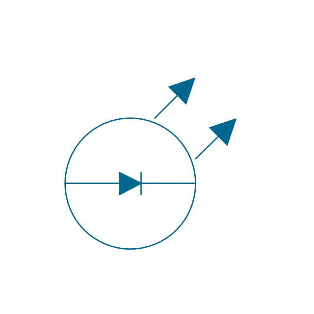
Diode, env
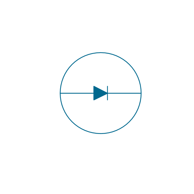
Diode

Diode, reverse blocking, env

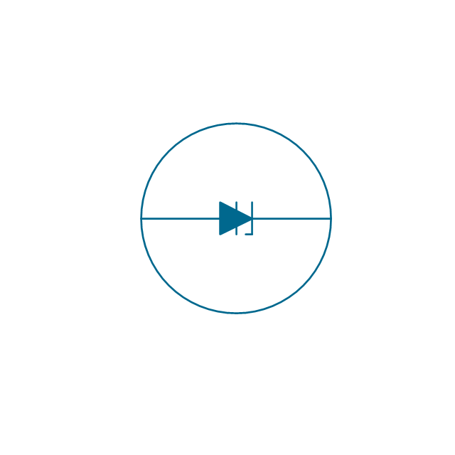
Diode, reverse blocking

Diode, reverse conducting, env
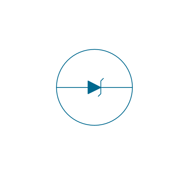
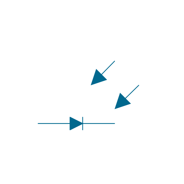
Diode, reverse conducting

Tunnel diode, env

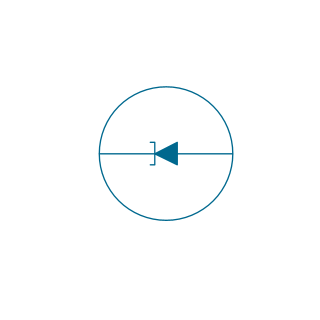
Tunnel diode

Zener diode, env
Zener diode

Backward diode, env
Backward diode

Varactor, env
Varactor
Four layer diode, env
Four layer diode
LED, env
LED
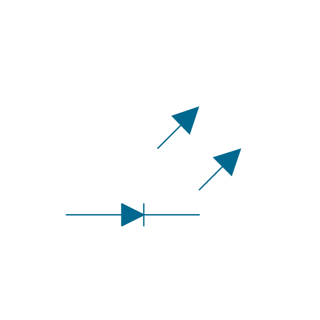
Photo-diode, env
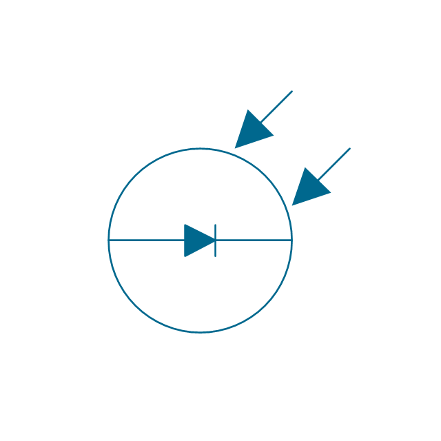
Photo-diode
Breakdown diode, uni-directional, env
Breakdown diode, uni-directional

Breakdown diode, bi-directional, env

Breakdown diode, bi-directional

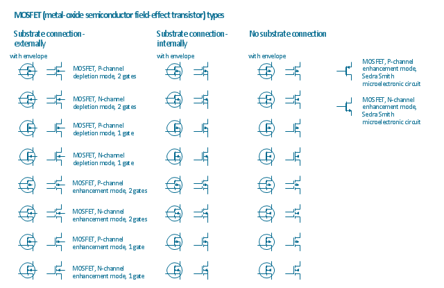
The vector stencils library "MOSFET" contains 18 symbols of MOSFET (metal–oxide–semiconductor field-effect transistor) elements for drawing electronic circuits diagrams.
"A variety of symbols are used for the MOSFET. The basic design is generally a line for the channel with the source and drain leaving it at right angles and then bending back at right angles into the same direction as the channel. Sometimes three line segments are used for enhancement mode and a solid line for depletion mode. ... Another line is drawn parallel to the channel for the gate.
The "bulk" or "body" connection, if shown, is shown connected to the back of the channel with an arrow indicating PMOS or NMOS. Arrows always point from P to N, so an NMOS (N-channel in P-well or P-substrate) has the arrow pointing in (from the bulk to the channel). If the bulk is connected to the source (as is generally the case with discrete devices) it is sometimes angled to meet up with the source leaving the transistor. If the bulk is not shown (as is often the case in IC design as they are generally common bulk) an inversion symbol is sometimes used to indicate PMOS, alternatively an arrow on the source may be used in the same way as for bipolar transistors (out for nMOS, in for pMOS). ...
For the symbols in which the bulk, or body, terminal is shown, it is here shown internally connected to the source... This is a typical configuration, but by no means the only important configuration. In general, the MOSFET is a four-terminal device, and in integrated circuits many of the MOSFETs share a body connection, not necessarily connected to the source terminals of all the transistors." [MOSFET. Wikipedia]
The symbols example "Design elements - MOSFET" was drawn using the ConceptDraw PRO diagramming and vector drawing software extended with the Electrical Engineering solution from the Engineering area of ConceptDraw Solution Park.
MOSFET symbols
- Electrical Symbols — Semiconductor | Electrical Symbols , Electrical ...
- Electrical Symbols — Semiconductor Diodes | Design elements ...
- Electrical Symbols , Electrical Diagram Symbols | Electrical Symbols ...
- Electrical Symbols — Semiconductor | Electrical Symbols ...
- Electrical Symbols — Semiconductor | Electrical Symbols ...
- Electrical Symbols — Semiconductor Diodes | Electrical Symbols ...
- Symbol For Semiconductor Diode
- Diagram Or Symbol Of Semiconductor
- Design elements - Semiconductor diodes | Electrical Drawing ...
- Electrical Symbols — Semiconductor Diodes | Electrical Symbols ...
- Electrical Symbols — Semiconductor Diodes | Semiconductor ...
- Design elements - Semiconductor diodes | Electrical Symbols ...
- Electrical Symbols — Semiconductor | Design elements ...
- Electrical Symbols — Semiconductor Diodes | Electrical Symbols ...
- Electrical Symbols — Semiconductor | Semiconductors - Vector ...
- Electrical Symbols — Semiconductor Diodes | Electrical Symbols ...
- All Symbol Of Semiconductor Pdf
- Electrical Symbols — Semiconductor | Electrical Symbols , Electrical ...
- Electrical Symbols — Semiconductor | Electrical Symbols ...
- Design elements - Semiconductor diodes | Swim Lane Flowchart ...