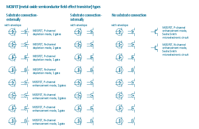
The vector stencils library "MOSFET" contains 18 symbols of MOSFET (metal–oxide–semiconductor field-effect transistor) elements for drawing electronic circuits diagrams.
"A variety of symbols are used for the MOSFET. The basic design is generally a line for the channel with the source and drain leaving it at right angles and then bending back at right angles into the same direction as the channel. Sometimes three line segments are used for enhancement mode and a solid line for depletion mode. ... Another line is drawn parallel to the channel for the gate.
The "bulk" or "body" connection, if shown, is shown connected to the back of the channel with an arrow indicating PMOS or NMOS. Arrows always point from P to N, so an NMOS (N-channel in P-well or P-substrate) has the arrow pointing in (from the bulk to the channel). If the bulk is connected to the source (as is generally the case with discrete devices) it is sometimes angled to meet up with the source leaving the transistor. If the bulk is not shown (as is often the case in IC design as they are generally common bulk) an inversion symbol is sometimes used to indicate PMOS, alternatively an arrow on the source may be used in the same way as for bipolar transistors (out for nMOS, in for pMOS). ...
For the symbols in which the bulk, or body, terminal is shown, it is here shown internally connected to the source... This is a typical configuration, but by no means the only important configuration. In general, the MOSFET is a four-terminal device, and in integrated circuits many of the MOSFETs share a body connection, not necessarily connected to the source terminals of all the transistors." [MOSFET. Wikipedia]
The symbols example "Design elements - MOSFET" was drawn using the ConceptDraw PRO diagramming and vector drawing software extended with the Electrical Engineering solution from the Engineering area of ConceptDraw Solution Park.
MOSFET symbols
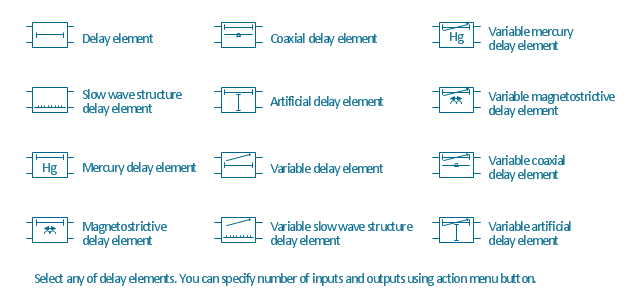
The vector stencils library "Delay elements" contains 12 symbols of delay elements for drawing electrical schematics and electronic circuit diagrams.
"An analog delay line is a network of electrical components connected in series, where each individual element creates a time difference or phase change between its input signal and its output signal. It operates on analog signals whose amplitude varies continuously. An example is a bucket-brigade device. Other types of delay line include acoustic, magnetostrictive, and surface acoustic wave devices. A series of RC networks can be cascaded to form a delay. A long transmission line can also provide a delay element. The delay time of an analog delay line may be only a few nanoseconds or several milliseconds, limited by the practical size of the physical medium used to delay the signal and the propagation speed of impulses in the medium." [Analog delay line. Wikipedia]
The symbols example "Design elements - Delay elements" was drawn using the ConceptDraw PRO diagramming and vector drawing software extended with the Electrical Engineering solution from the Engineering area of ConceptDraw Solution Park.
Delay element symbols
- Symbols Used In Line Design
- Design elements - Delay elements | Line Symbol Of Electrical Impulse
- Entity Relationship Diagram Symbols | ERD Symbols and Meanings ...
- Which Component Used For Delay Line Draw The Symbol
- Design elements - Delay elements | Basic Flowchart Symbols and ...
- Design elements - Delay elements | Electrical Symbols , Electrical ...
- Symbols Used In Engineering Lines
- Power Transmission Line Symbols Used
- Entity Relationship Diagram - ERD - Software for Design Crows Foot ...
- Engineering Line Symbol
- What Are The Symbols Used In Line Design
- Interior Design Site Plan - Design Elements | Graphical Symbols ...
- Design elements - ER diagram (Chen notation) | Chen Notation ...
- Symbols For Transmission Line Diagram
- Electrical Symbols — Transmission Paths | Design elements ...
- Process Line Symbols
- Basic Flowchart Symbols and Meaning | Audit Flowchart Symbols ...
- ERD Symbols and Meanings | Components of ER Diagram | Entity ...
- Basic Flowchart Symbols and Meaning | Flowchart design ...
- Basic Flowchart Symbols and Meaning | In Bpmn Notation A Solid ...
- ERD | Entity Relationship Diagrams, ERD Software for Mac and Win
- Flowchart | Basic Flowchart Symbols and Meaning
- Flowchart | Flowchart Design - Symbols, Shapes, Stencils and Icons
- Flowchart | Flow Chart Symbols
- Electrical | Electrical Drawing - Wiring and Circuits Schematics
- Flowchart | Common Flowchart Symbols
- Flowchart | Common Flowchart Symbols