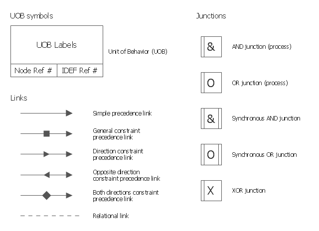
The vector stencils library "IDEF3 process schematic symbols" contains 12 shapes: unit of behavior (UOB), links, junctions, .
Use it to design your IDEF3 process schematic diagrams.
"Process schematics tend to be the most familiar and broadly used component of the IDEF3 method. These schematics provide a visualization mechanism for processcentered descriptions of a scenario. The graphical elements that comprise process schematics include Unit of Behavior (UOB) boxes, precedence links, junctions, referents, and notes. The building blocks here are:
- Unit of Behavior (UOB) boxes.
- Links: Links are the glue that connect UOB boxes to form representations of dynamic processes.
- Simple Precedence Links: Precedence links express temporal precedence relations between instances of one UOB and those of another.
- Activation Plots: Activation plots are used to represent activations.
- Dashed Links: Dashed links carry no predefined semantics.
- Link Numbers: All links have an elaboration and unique link numbers.
Activation Semantics for Nonbranching Process Schematics.
- Junctions: Junctions in IDEF3 provide a mechanism to specify the logic of process branching.
- UOB Decompositions: Elaborations capture and structure detailed knowledge about processes.
- UOB Reference Numbering Scheme: A UOB box number is assigned to each UOB box in an IDEF3 Process Description.
- Partial Descriptions: UOB boxes are joined together by links. Because of the description capture focus of IDEF3, it is possible to conceive of UOBs without links to other parts of an IDEF3 schematic.
- Referents: Referents enhance understanding, provide additional meaning, and simplify the construction (i.e., minimize clutter) of both process schematics and object schematics." [IDEF3. Wikipedia]
The shapes example "Design elements - IDEF3 process schematic symbols" was created using the ConceptDraw PRO diagramming and vector drawing software extended with the solution "IDEF Business Process Diagrams" from the area "Business Processes" of ConceptDraw Solution Park.
IDEF3 business process diagram
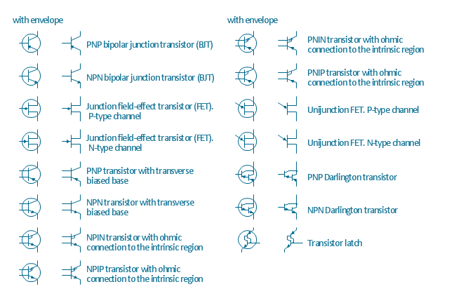
The vector stencils library "Transistors" contains 30 symbols of transistors drawing electronic schematics and circuit diagrams.
"A transistor is a semiconductor device used to amplify and switch electronic signals and electrical power. It is composed of semiconductor material with at least three terminals for connection to an external circuit. A voltage or current applied to one pair of the transistor's terminals changes the current through another pair of terminals. Because the controlled (output) power can be higher than the controlling (input) power, a transistor can amplify a signal. Today, some transistors are packaged individually, but many more are found embedded in integrated circuits.
The transistor is the fundamental building block of modern electronic devices, and is ubiquitous in modern electronic systems. ...
Transistors are categorized by:
(1) Semiconductor material...: the metalloids germanium ... and silicon ... in amorphous, polycrystalline and monocrystalline form; the compounds gallium arsenide ... and silicon carbide ..., the alloy silicon-germanium ..., the allotrope of carbon graphene ...
(2) Structure: BJT, JFET, IGFET (MOSFET), insulated-gate bipolar transistor, "other types"
(3) Electrical polarity (positive and negative): n–p–n, p–n–p (BJTs); n-channel, p-channel (FETs)
(4) Maximum power rating: low, medium, high
(5) Maximum operating frequency: low, medium, high, radio (RF), microwave frequency...
(6) Application: switch, general purpose, audio, high voltage, super-beta, matched pair
(7) Physical packaging: through-hole metal, through-hole plastic, surface mount, ball grid array, power modules...
(8) Amplification factor..." [Transistor. Wikipedia]
The shapes example "Design elements - Transistors" was drawn using the ConceptDraw PRO diagramming and vector drawing software extended with the Electrical Engineering solution from the Engineering area of ConceptDraw Solution Park.
Transistor symbols
- Block Diagram | Basic Flowchart Symbols and Meaning | UML Block ...
- Vector stencils library - IDEF3 process schematic symbols | Vector ...
- Symbol Block Diagram Of Communication Circuit
- UML Block Diagram | Block Diagram | Electrical Symbols , Electrical ...
- Basic Flowchart Symbols and Meaning | Data Flow Diagram ...
- Electrical Symbols Com
- Electrical Drawing Software and Electrical Symbols
- Electrical Symbols , Electrical Schematic Symbols | Electrical ...
- Basic Flowchart Symbols and Meaning | Process Flowchart | Block ...
- DFD Library System | Functional Block Diagram | Block Diagram ...
- Electrical Block Diagram Website
- Mechanical Drawing Symbols | Electrical Symbols , Electrical ...
- Electrical Diagram Symbols | Electrical Drawing Software | How To ...
- Process Flowchart | Electrical Drawing Software and Electrical ...
- Entity Relationship Diagram Symbols | Basic Flowchart Symbols and ...
- Function Block Diagram Examples
- Mechanical Engineering | Electrical Drawing Software and Electrical ...
- Block Diagram Creator | Process Flowchart | Design elements ...
- Basic Flowchart Symbols and Meaning | Process Flowchart ...
- Piping and Instrumentation Diagram Software | Electrical Symbols ...
- ERD | Entity Relationship Diagrams, ERD Software for Mac and Win
- Flowchart | Basic Flowchart Symbols and Meaning
- Flowchart | Flowchart Design - Symbols, Shapes, Stencils and Icons
- Flowchart | Flow Chart Symbols
- Electrical | Electrical Drawing - Wiring and Circuits Schematics
- Flowchart | Common Flowchart Symbols
- Flowchart | Common Flowchart Symbols