Electrical Symbols — Logic Gate Diagram

26 libraries of the Electrical Engineering Solution of ConceptDraw PRO make your electrical diagramming simple, efficient, and effective. You can simply and quickly drop the ready-to-use objects from libraries into your document to create the electrical diagram.
"A logic gate is an idealized or physical device implementing a Boolean function, that is, it performs a logical operation on one or more logical inputs, and produces a single logical output. Depending on the context, the term may refer to an ideal logic gate, one that has for instance zero rise time and unlimited fan-out, or it may refer to a non-ideal physical device...
Logic gates are primarily implemented using diodes or transistors acting as electronic switches, but can also be constructed using electromagnetic relays (relay logic), fluidic logic, pneumatic logic, optics, molecules, or even mechanical elements. With amplification, logic gates can be cascaded in the same way that Boolean functions can be composed, allowing the construction of a physical model of all of Boolean logic, and therefore, all of the algorithms and mathematics that can be described with Boolean logic.
Logic circuits include such devices as multiplexers, registers, arithmetic logic units (ALUs), and computer memory, all the way up through complete microprocessors, which may contain more than 100 million gates. In practice, the gates are made from field-effect transistors (FETs), particularly MOSFETs (metal–oxide–semiconductor field-effect transistors).
Compound logic gates AND-OR-Invert (AOI) and OR-AND-Invert (OAI) are often employed in circuit design because their construction using MOSFETs is simpler and more efficient than the sum of the individual gates.
In reversible logic, Toffoli gates are used." [Logic gate. Wikipedia]
The logic gate diagram template for the ConceptDraw PRO diagramming and vector drawing software is included in the Electrical Engineering solution from the Engineering area of ConceptDraw Solution Park.
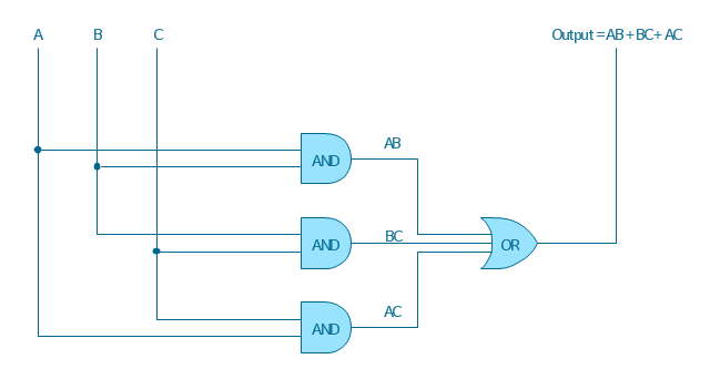
Logic gate diagram
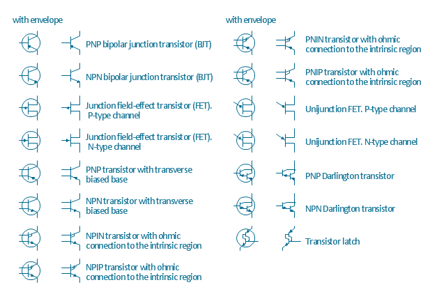
The vector stencils library "Transistors" contains 30 symbols of transistors drawing electronic schematics and circuit diagrams.
"A transistor is a semiconductor device used to amplify and switch electronic signals and electrical power. It is composed of semiconductor material with at least three terminals for connection to an external circuit. A voltage or current applied to one pair of the transistor's terminals changes the current through another pair of terminals. Because the controlled (output) power can be higher than the controlling (input) power, a transistor can amplify a signal. Today, some transistors are packaged individually, but many more are found embedded in integrated circuits.
The transistor is the fundamental building block of modern electronic devices, and is ubiquitous in modern electronic systems. ...
Transistors are categorized by:
(1) Semiconductor material...: the metalloids germanium ... and silicon ... in amorphous, polycrystalline and monocrystalline form; the compounds gallium arsenide ... and silicon carbide ..., the alloy silicon-germanium ..., the allotrope of carbon graphene ...
(2) Structure: BJT, JFET, IGFET (MOSFET), insulated-gate bipolar transistor, "other types"
(3) Electrical polarity (positive and negative): n–p–n, p–n–p (BJTs); n-channel, p-channel (FETs)
(4) Maximum power rating: low, medium, high
(5) Maximum operating frequency: low, medium, high, radio (RF), microwave frequency...
(6) Application: switch, general purpose, audio, high voltage, super-beta, matched pair
(7) Physical packaging: through-hole metal, through-hole plastic, surface mount, ball grid array, power modules...
(8) Amplification factor..." [Transistor. Wikipedia]
The shapes example "Design elements - Transistors" was drawn using the ConceptDraw PRO diagramming and vector drawing software extended with the Electrical Engineering solution from the Engineering area of ConceptDraw Solution Park.
Transistor symbols
- Compound Gate Design Diagram
- Electrical Symbols — Resistors | Electrical Symbols — Logic Gate ...
- Electrical Symbols — Logic Gate Diagram | Design elements - Logic ...
- Design elements - Logic gate diagram | Circuits and Logic Diagram ...
- Design elements - Logic gate diagram
- Design elements - Logic gate diagram | Electrical Symbols ...
- Design elements - Logic gate diagram | Logic gate diagram ...
- Circuits and Logic Diagram Software | Logic gate diagram ...
- Logic gate diagram - Template | Electrical Symbols, Electrical ...
- Logic gate diagram - Template | Circuits and Logic Diagram ...
- Logic gate diagram - Template | Venn Diagram Template for Word ...
- Venn Diagram Examples for Problem Solving. Venn Diagram as a ...
- Gate Design Software
- Logic gate diagram - Template | Engineering | Electrical Symbols ...
- Logic gate diagram - Template | Electrical Symbols — Logic Gate ...
- Electrical Drafting And Design Logic Gate
- Design elements - Logic gate diagram | 2-bit ALU - Logic gate ...
- Circuits and Logic Diagram Software | Electrical Symbols — Logic ...
- Circuits and Logic Diagram Software | Design elements - Logic gate ...
- 2-bit ALU - Logic gate diagram
- ERD | Entity Relationship Diagrams, ERD Software for Mac and Win
- Flowchart | Basic Flowchart Symbols and Meaning
- Flowchart | Flowchart Design - Symbols, Shapes, Stencils and Icons
- Flowchart | Flow Chart Symbols
- Electrical | Electrical Drawing - Wiring and Circuits Schematics
- Flowchart | Common Flowchart Symbols
- Flowchart | Common Flowchart Symbols