Electrical Symbols — MOSFET

Although the MOSFET is a four-terminal device with source (S), gate (G), drain (D), and body (B) terminals, the body (or substrate) of the MOSFET is often connected to the source terminal, making it a three-terminal device like other field-effect transistors. Because these two terminals are normally connected to each other (short-circuited) internally, only three terminals appear in electrical diagrams. The MOSFET is by far the most common transistor in both digital and analog circuits, though the bipolar junction transistor was at one time much more common.
26 libraries of the Electrical Engineering Solution of ConceptDraw DIAGRAM make your electrical diagramming simple, efficient, and effective. You can simply and quickly drop the ready-to-use objects from libraries into your document to create the electrical diagram.
Electrical Symbols — IGFET

The early term metal oxide semiconductor field-effect transistor (MOSFET) is still in
use, and MOSFET is usually acceptable as a generic term for IGFETs. The metal oxide, and the insulation in the IGFET, is the insulating material between the gate terminal and the substrate between the source and drain terminals. This insulator must have very low leakage, of course, but another requirement for good performance of the transistor is that the dielectric constant of the material must be very high.
26 libraries of the Electrical Engineering Solution of ConceptDraw DIAGRAM make your electrical diagramming simple, efficient, and effective. You can simply and quickly drop the ready-to-use objects from libraries into your document to create the electrical diagram.
Electrical Symbols — Semiconductor

26 libraries of the Electrical Engineering Solution of ConceptDraw DIAGRAM make your electrical diagramming simple, efficient, and effective. You can simply and quickly drop the ready-to-use objects from libraries into your document to create the electrical diagram.
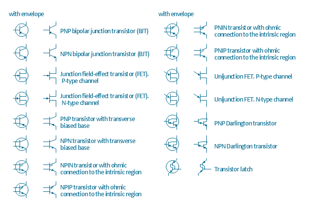
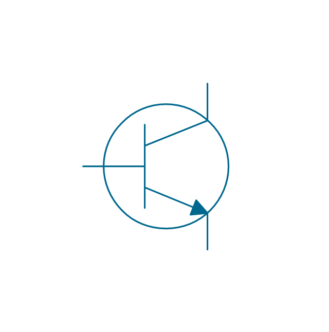
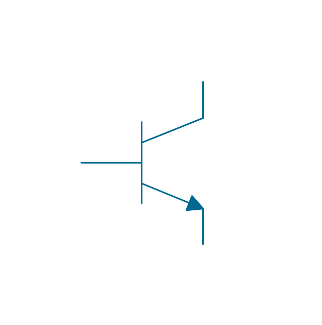
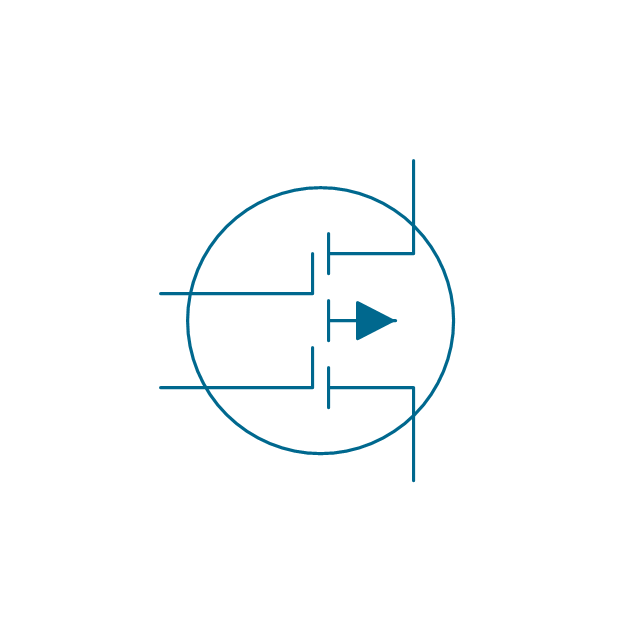
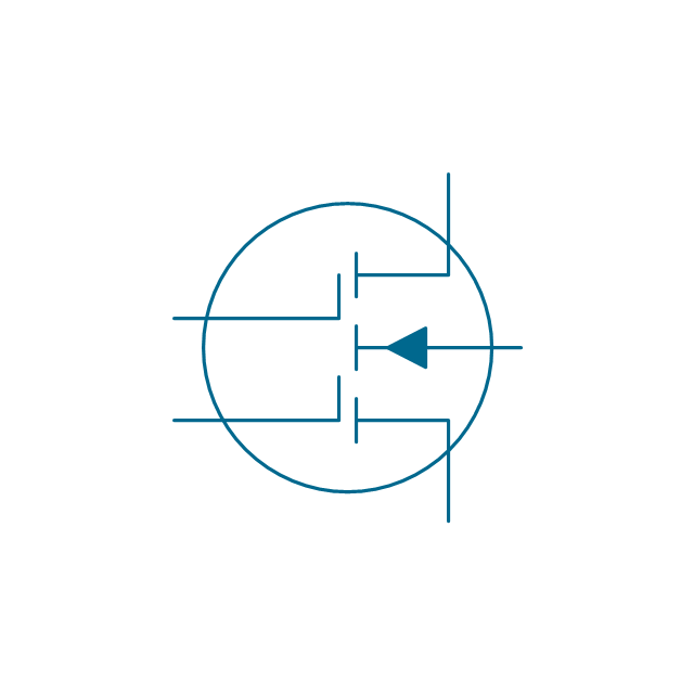
Electrical Symbols — Transistors

26 libraries of the Electrical Engineering Solution of ConceptDraw DIAGRAM make your electrical diagramming simple, efficient, and effective. You can simply and quickly drop the ready-to-use objects from libraries into your document to create the electrical diagram.
The vector stencils library "Transistors" contains 30 symbols of transistors drawing electronic schematics and circuit diagrams.
"A transistor is a semiconductor device used to amplify and switch electronic signals and electrical power. It is composed of semiconductor material with at least three terminals for connection to an external circuit. A voltage or current applied to one pair of the transistor's terminals changes the current through another pair of terminals. Because the controlled (output) power can be higher than the controlling (input) power, a transistor can amplify a signal. Today, some transistors are packaged individually, but many more are found embedded in integrated circuits.
The transistor is the fundamental building block of modern electronic devices, and is ubiquitous in modern electronic systems. ...
Transistors are categorized by:
(1) Semiconductor material...: the metalloids germanium ... and silicon ... in amorphous, polycrystalline and monocrystalline form; the compounds gallium arsenide ... and silicon carbide ..., the alloy silicon-germanium ..., the allotrope of carbon graphene ...
(2) Structure: BJT, JFET, IGFET (MOSFET), insulated-gate bipolar transistor, "other types"
(3) Electrical polarity (positive and negative): n–p–n, p–n–p (BJTs); n-channel, p-channel (FETs)
(4) Maximum power rating: low, medium, high
(5) Maximum operating frequency: low, medium, high, radio (RF), microwave frequency...
(6) Application: switch, general purpose, audio, high voltage, super-beta, matched pair
(7) Physical packaging: through-hole metal, through-hole plastic, surface mount, ball grid array, power modules...
(8) Amplification factor..." [Transistor. Wikipedia]
The shapes example "Design elements - Transistors" was drawn using the ConceptDraw PRO diagramming and vector drawing software extended with the Electrical Engineering solution from the Engineering area of ConceptDraw Solution Park.
Transistor symbols
Wiring Diagrams with ConceptDraw DIAGRAM

ERD Symbols and Meanings

The Chen's ERD notation is still used and is considered to present a more detailed way of representing entities and relationships.
To create an ERD, software engineers mainly turn to dedicated drawing software, which contain the full notation resources for their specific database design - ERD symbols and meanings. CS Odessa has released an all-inclusive Entity-Relationship Diagram (ERD) solution for their powerful drawing program, ConceptDraw DIAGRAM.

Process Flow Chart Symbols

It is incredibly convenient to use the ConceptDraw DIAGRAM software extended with Flowcharts Solution from the "Diagrams" Area of ConceptDraw Solution Park for designing professional looking Process Flow Charts.
Electrical Symbols, Electrical Diagram Symbols

This solution provides 26 libraries which contain 926 electrical symbols from electrical engineering: Analog and Digital Logic, Composite Assemblies, Delay Elements, Electrical Circuits, Electron Tubes, IGFET, Inductors, Integrated Circuit, Lamps, Acoustics, Readouts, Logic Gate Diagram, MOSFET, Maintenance, Power Sources, Qualifying, Resistors, Rotating Equipment, Semiconductor Diodes, Semiconductors, Stations, Switches and Relays, Terminals and Connectors, Thermo, Transformers and Windings, Transistors, Transmission Paths,VHF UHF SHF.
Electrical Symbols — Integrated Circuit

26 libraries of the Electrical Engineering Solution of ConceptDraw DIAGRAM make your electrical diagramming simple, efficient, and effective. You can simply and quickly drop the ready-to-use objects from libraries into your document to create the electrical diagram.
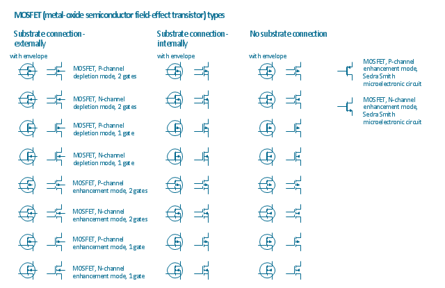
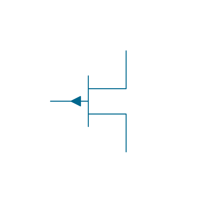
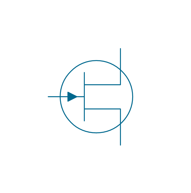
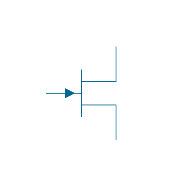
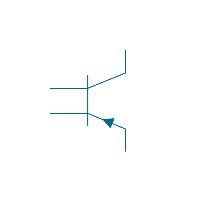
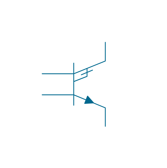
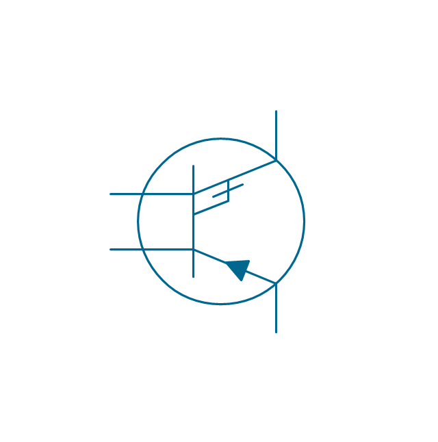
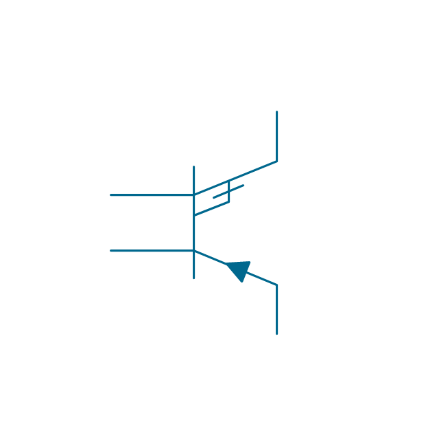
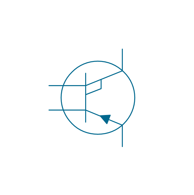
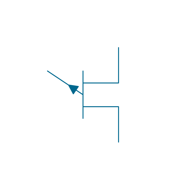
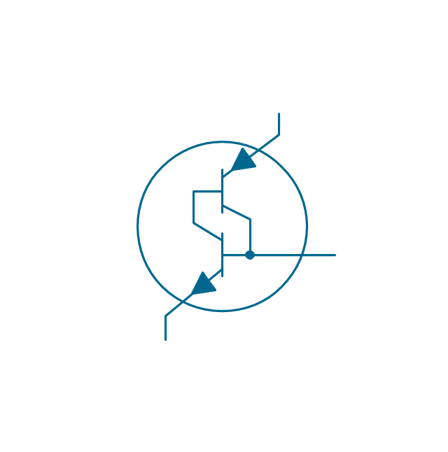
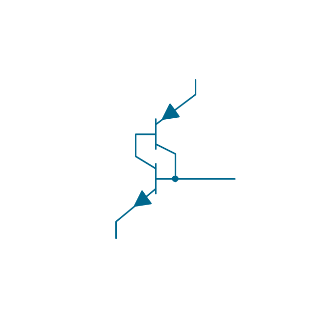
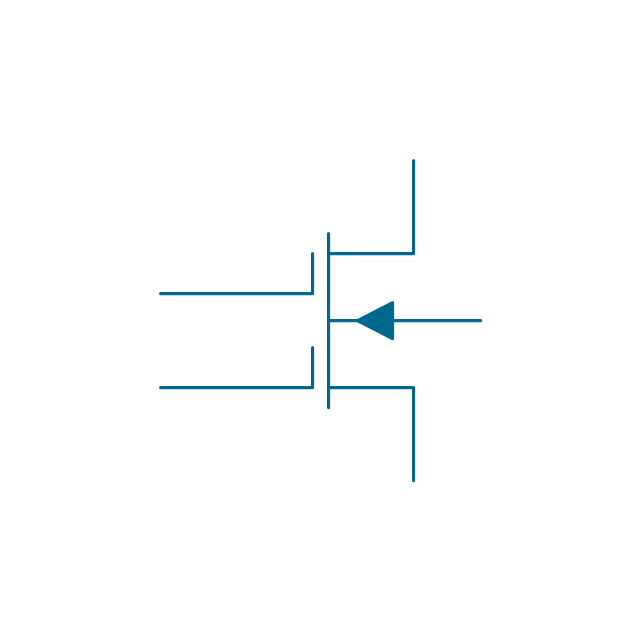
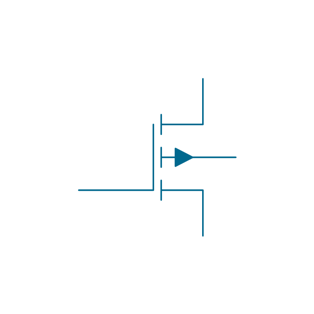
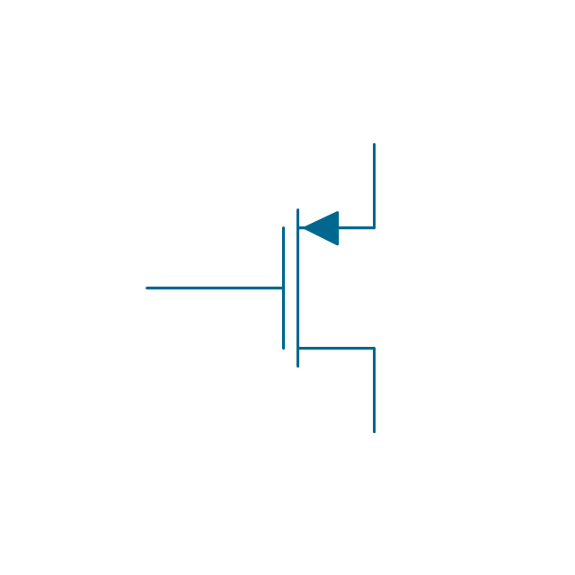
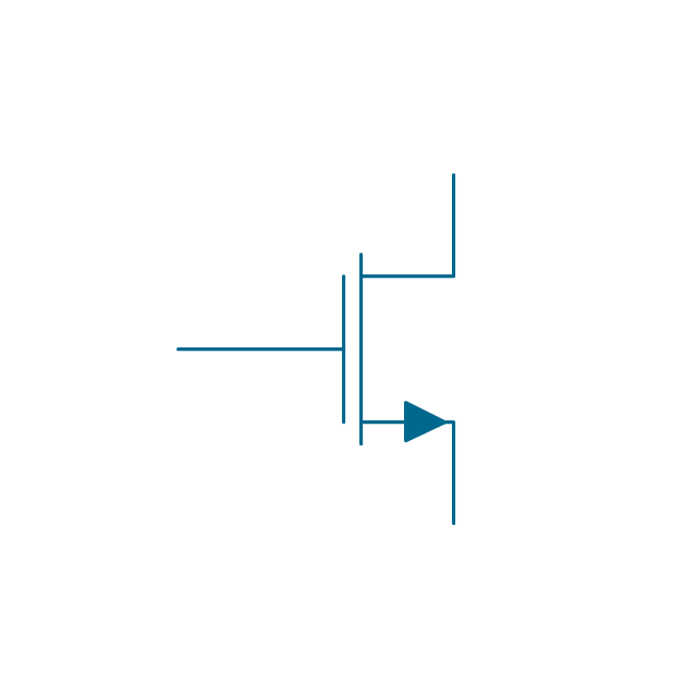
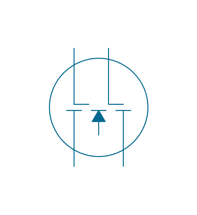
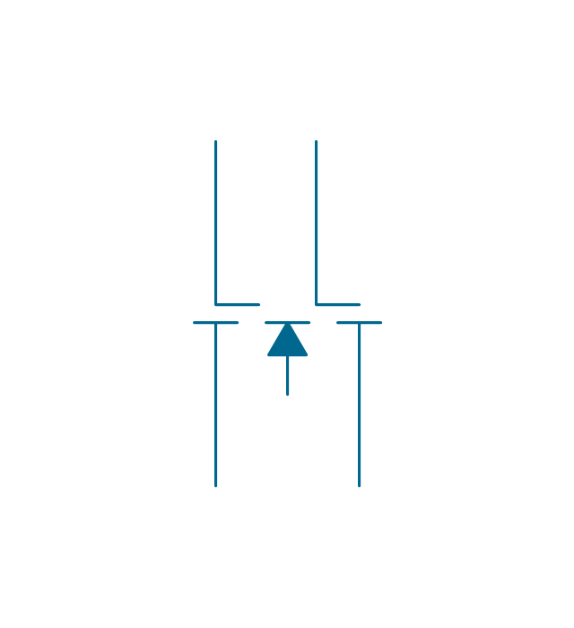
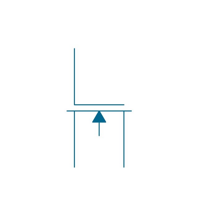
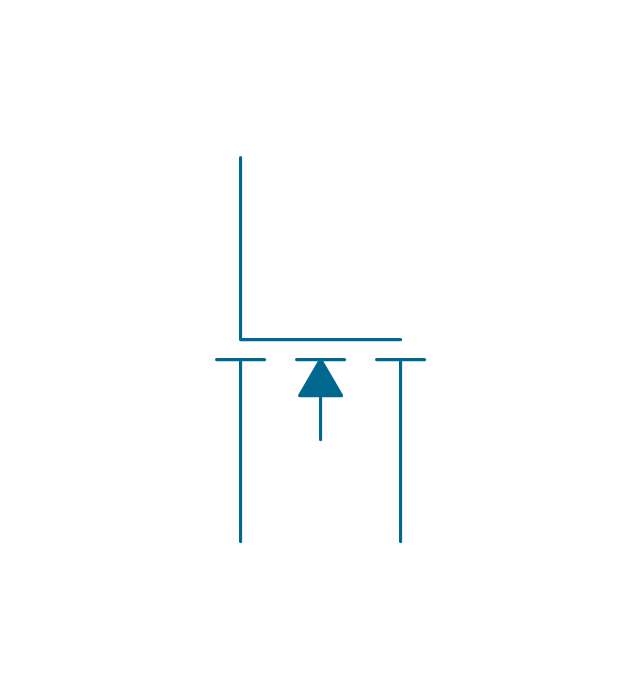
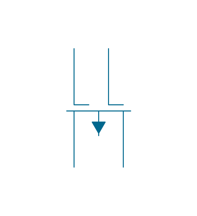
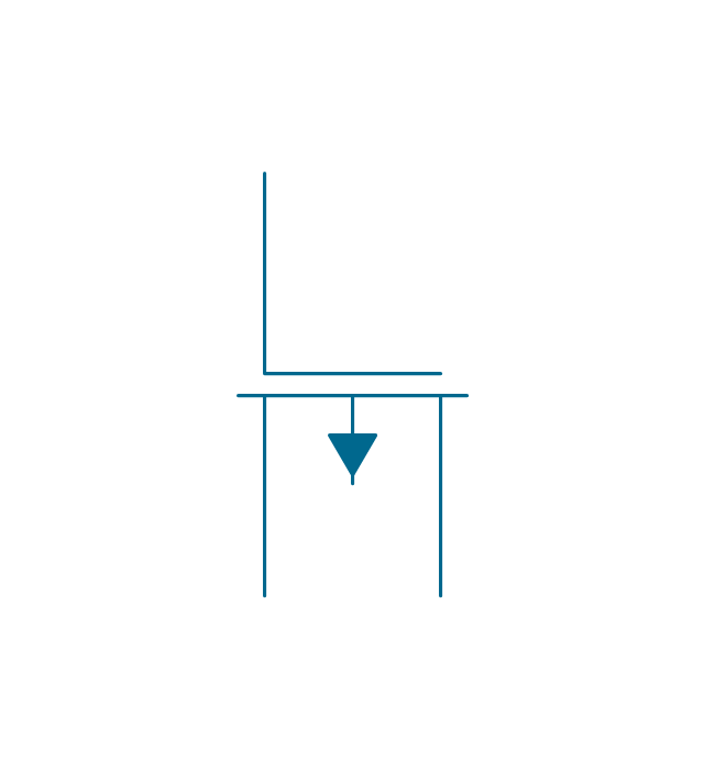
The vector stencils library "MOSFET" contains 18 symbols of MOSFET (metal–oxide–semiconductor field-effect transistor) elements for drawing electronic circuits diagrams.
"A variety of symbols are used for the MOSFET. The basic design is generally a line for the channel with the source and drain leaving it at right angles and then bending back at right angles into the same direction as the channel. Sometimes three line segments are used for enhancement mode and a solid line for depletion mode. ... Another line is drawn parallel to the channel for the gate.
The "bulk" or "body" connection, if shown, is shown connected to the back of the channel with an arrow indicating PMOS or NMOS. Arrows always point from P to N, so an NMOS (N-channel in P-well or P-substrate) has the arrow pointing in (from the bulk to the channel). If the bulk is connected to the source (as is generally the case with discrete devices) it is sometimes angled to meet up with the source leaving the transistor. If the bulk is not shown (as is often the case in IC design as they are generally common bulk) an inversion symbol is sometimes used to indicate PMOS, alternatively an arrow on the source may be used in the same way as for bipolar transistors (out for nMOS, in for pMOS). ...
For the symbols in which the bulk, or body, terminal is shown, it is here shown internally connected to the source... This is a typical configuration, but by no means the only important configuration. In general, the MOSFET is a four-terminal device, and in integrated circuits many of the MOSFETs share a body connection, not necessarily connected to the source terminals of all the transistors." [MOSFET. Wikipedia]
The symbols example "Design elements - MOSFET" was drawn using the ConceptDraw PRO diagramming and vector drawing software extended with the Electrical Engineering solution from the Engineering area of ConceptDraw Solution Park.
MOSFET symbols
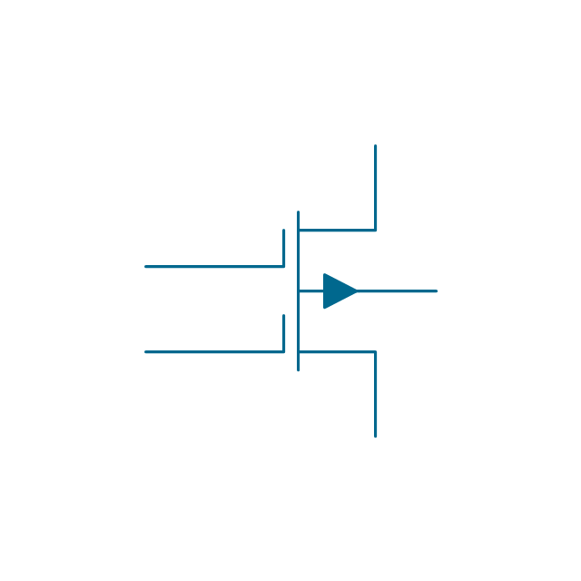
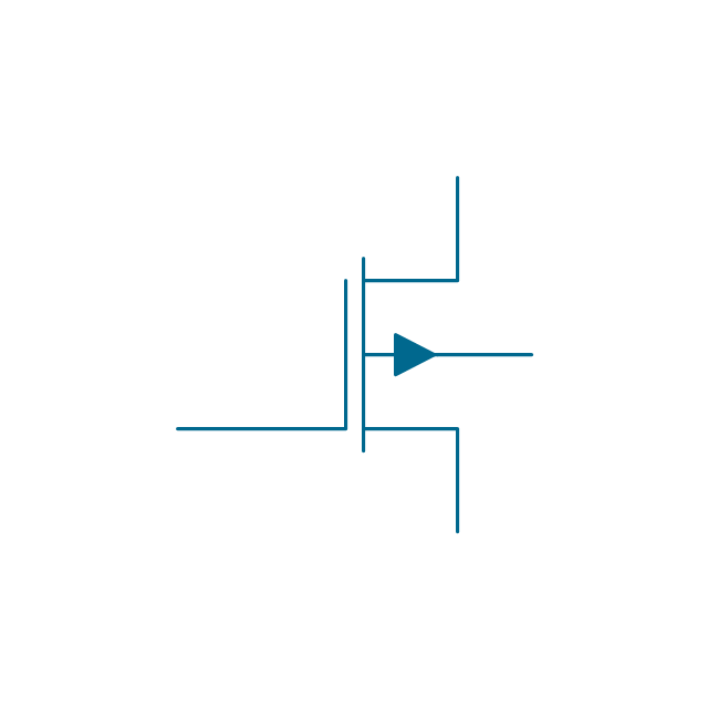
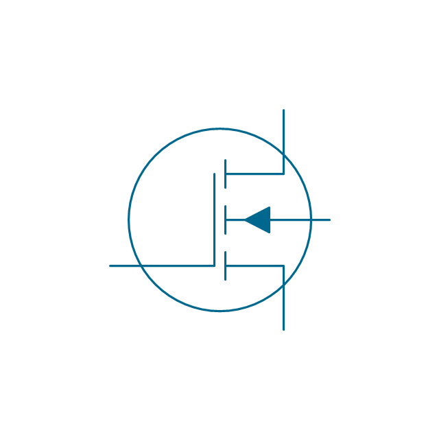
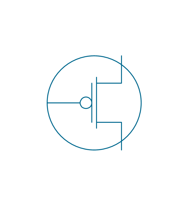
The vector stencils library "IGFET" contains 18 symbols of IGFET (insulated-gate field-effect transistor) elements for drawing electronic circuit diagrams.
"The metal–oxide–semiconductor field-effect transistor (MOSFET, MOS-FET, or MOS FET) is a transistor used for amplifying or switching electronic signals. Although the MOSFET is a four-terminal device with source (S), gate (G), drain (D), and body (B) terminals, the body (or substrate) of the MOSFET often is connected to the source terminal, making it a three-terminal device like other field-effect transistors. Because these two terminals are normally connected to each other (short-circuited) internally, only three terminals appear in electrical diagrams. The MOSFET is by far the most common transistor in both digital and analog circuits, though the bipolar junction transistor was at one time much more common. ...
An insulated-gate field-effect transistor or IGFET is a related term almost synonymous with MOSFET. The term may be more inclusive, since many "MOSFETs" use a gate that is not metal, and a gate insulator that is not oxide. Another synonym is MISFET for metal–insulator–semiconductor FET." [MOSFET
From Wikipedia]
The symbols example "Design elements - IGFET" was drawn using the ConceptDraw PRO diagramming and vector drawing software extended with the Electrical Engineering solution from the Engineering area of ConceptDraw Solution Park.
IGFET elements

How To use House Electrical Plan Software

You can use many of built-in templates, electrical symbols and electical schemes examples of our House Electrical Diagram Software.
ConceptDraw is a fast way to draw: Electrical circuit diagrams, Schematics, Electrical Wiring, Circuit schematics, Digital circuits, Wiring in buildings, Electrical equipment, House electrical plans, Home cinema, Satellite television, Cable television, Closed-circuit television.
House Electrical Plan Software works across any platform, meaning you never have to worry about compatibility again. ConceptDraw DIAGRAM allows you to make electrical circuit diagrams on PC or macOS operating systems.

Electrical Diagram Software

Electrical Engineering Solution for ConceptDraw DIAGRAM provides the 26 stencils libraries of ready-to-use predesigned vector symbols, templates and samples that make your electrical drawing quick, easy and effective.
The vector stencils library "Transistors" contains 30 symbols of transistors.
Use these shapes for drawing electronic schematics and circuit diagrams in the ConceptDraw PRO diagramming and vector drawing software extended with the Electrical Engineering solution from the Engineering area of ConceptDraw Solution Park.
www.conceptdraw.com/ solution-park/ engineering-electrical
Use these shapes for drawing electronic schematics and circuit diagrams in the ConceptDraw PRO diagramming and vector drawing software extended with the Electrical Engineering solution from the Engineering area of ConceptDraw Solution Park.
www.conceptdraw.com/ solution-park/ engineering-electrical
BJT, PNP, env
BJT, PNP
BJT, NPN, env
BJT, NPN
JFET, P, env

JFET, P
JFET, N, env
JFET, N
Transverse biased base, PNP, env

Transverse biased base, PNP
Transverse biased base, NPN, env

Transverse biased base, NPN

Ohmic, NPIN, env
Ohmic, NPIN

Ohmic, NPIP, env
Ohmic, NPIP
Ohmic, PNIN, env
Ohmic, PNIN
Ohmic, PNIP, env
Ohmic, PNIP

Unijunction FET, P, env

Unijunction FET, P
Unijunction FET, N, env

Unijunction FET, N

Darlington transistor, PNP, env
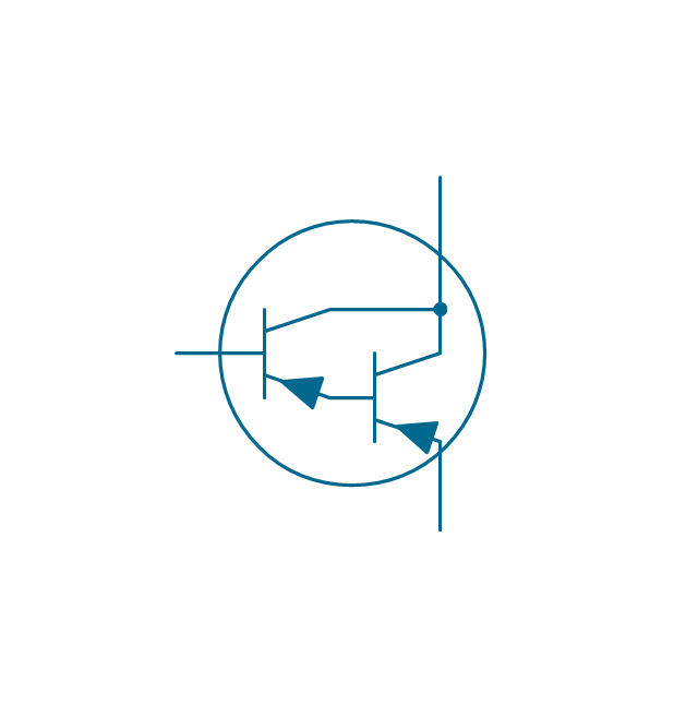
Darlington transistor, PNP
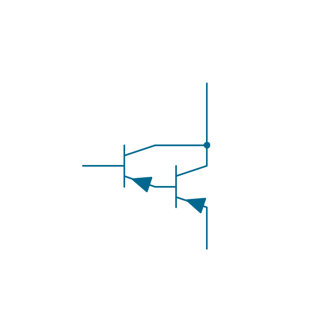
Darlington transistor, NPN, env
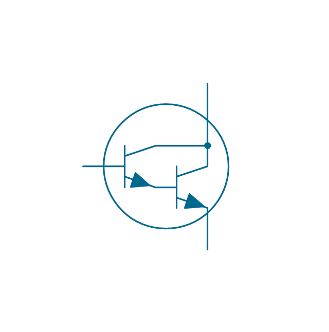
Darlington transistor, NPN

Transistor latch, env
Transistor latch
The vector stencils library "Logic gate diagram" contains 17 element symbols for drawing the logic gate diagrams.
"To build a functionally complete logic system, relays, valves (vacuum tubes), or transistors can be used. The simplest family of logic gates using bipolar transistors is called resistor-transistor logic (RTL). Unlike simple diode logic gates (which do not have a gain element), RTL gates can be cascaded indefinitely to produce more complex logic functions. RTL gates were used in early integrated circuits. For higher speed and better density, the resistors used in RTL were replaced by diodes resulting in diode-transistor logic (DTL). Transistor-transistor logic (TTL) then supplanted DTL. As integrated circuits became more complex, bipolar transistors were replaced with smaller field-effect transistors (MOSFETs); see PMOS and NMOS. To reduce power consumption still further, most contemporary chip implementations of digital systems now use CMOS logic. CMOS uses complementary (both n-channel and p-channel) MOSFET devices to achieve a high speed with low power dissipation." [Logic gate. Wikipedia]
The symbols example "Design elements - Logic gate diagram" was drawn using the ConceptDraw PRO diagramming and vector drawing software extended with the Electrical Engineering solution from the Engineering area of ConceptDraw Solution Park.
Logic gate symbols
Electrical Symbols — Lamps, Acoustics, Readouts

26 libraries of the Electrical Engineering Solution of ConceptDraw DIAGRAM make your electrical diagramming simple, efficient, and effective. You can simply and quickly drop the ready-to-use objects from libraries into your document to create the electrical diagram.
The vector stencils library "MOSFET" contains 18 symbols of MOSFET (metal–oxide–semiconductor field-effect transistor) elements.
Use these shapes for drawing electronic circuits diagrams in the ConceptDraw PRO diagramming and vector drawing software extended with the Electrical Engineering solution from the Engineering area of ConceptDraw Solution Park.
www.conceptdraw.com/ solution-park/ engineering-electrical
Use these shapes for drawing electronic circuits diagrams in the ConceptDraw PRO diagramming and vector drawing software extended with the Electrical Engineering solution from the Engineering area of ConceptDraw Solution Park.
www.conceptdraw.com/ solution-park/ engineering-electrical
MOSFET, P, dep, 2 gates, env

MOSFET, P, dep, 2 gates
MOSFET, N, dep, 2 gates, env

MOSFET, N, dep, 2 gates
MOSFET, P, dep, 1 gate, env

MOSFET, P, dep, 1 gate
MOSFET, N, dep, 1 gate, env

MOSFET, N, dep, 1 gate

MOSFET, P, enh, 2 gates, env
MOSFET, P, enh, 2 gates

MOSFET, N, enh, 2 gates, env
MOSFET, N, enh, 2 gates

MOSFET, P, enh, 1 gate, env

MOSFET, P, enh, 1 gate
MOSFET, N, enh, 1 gate, env
MOSFET, N, enh, 1 gate

MOSFET, P, enh, Sedra
MOSFET, N, enh, Sedra
Mechanical Drawing Symbols

The vector stencils library "IGFET" contains 18 symbols of IGFET (insulated-gate field-effect transistor) elements.
Use these shapes for drawing electronic circuit diagrams in the ConceptDraw PRO diagramming and vector drawing software extended with the Electrical Engineering solution from the Engineering area of ConceptDraw Solution Park.
www.conceptdraw.com/ solution-park/ engineering-electrical
Use these shapes for drawing electronic circuit diagrams in the ConceptDraw PRO diagramming and vector drawing software extended with the Electrical Engineering solution from the Engineering area of ConceptDraw Solution Park.
www.conceptdraw.com/ solution-park/ engineering-electrical
IGFET, N, dep, 2 gates, env

IGFET, N, dep, 2 gates

IGFET, N, enh, 2 gates, env
IGFET, N, enh, 2 gates
IGFET, N, dep, 1 gate, env

IGFET, N, dep, 1 gate
IGFET, N, enh, 1 gate, env

IGFET, N, enh, 1 gate, env
IGFET, P, dep, 2 gates, env

IGFET, P, dep, 2 gates
IGFET, P, enh, 2 gates, env

IGFET, P, enh, 2 gates

IGFET, P, dep, 1 gate, env

IGFET, P, dep, 1 gate
IGFET, P, enh, 1 gate, env

IGFET, P, enh, 1 gate

IGFET, N, enh

IGFET, P, enh
- Electrical Symbols — Transistors | Electrical Symbols — MOSFET ...
- MOSFET
- MOSFET
- Oil Crude P
- Process Flow Diagram Symbols | Design elements - Heating ...
- Bipolar current mirror - Circuit diagram | Transistors - Vector stencils ...
- Design elements - Transistors | Design elements - MOSFET | Design ...
- How to Draw a Chemical Process Flow Diagram | How to Create a ...
- MOSFET - Vector stencils library | Design elements - IGFET | Design ...
- Electrical Symbols — Transistors | Design elements - Transistors ...
- Design elements - Logic gate diagram | Engineering | 2-bit ALU ...
- Piping and Instrumentation Diagram Software | Process Flow ...
- Semi Conductor Devices Diagram
- Amine treating unit schematic diagram
- Process Flow Diagram Symbols | Electrical Symbols — Analog and ...
- Electrical Symbols — Transistors | Design elements - Transistors ...
- Draw Symbols Of Different Compound Used In Electric Circuit
- Design elements - Logic gate diagram | Symbol Amplifier Diagram
- Design elements - MOSFET | Electrical Symbols — Switches and ...
- Circuit diagram - EL 34 schematics | Design elements - Electron ...
- ERD | Entity Relationship Diagrams, ERD Software for Mac and Win
- Flowchart | Basic Flowchart Symbols and Meaning
- Flowchart | Flowchart Design - Symbols, Shapes, Stencils and Icons
- Flowchart | Flow Chart Symbols
- Electrical | Electrical Drawing - Wiring and Circuits Schematics
- Flowchart | Common Flowchart Symbols
- Flowchart | Common Flowchart Symbols